ABOUT RAM

classic Classic list List threaded Threaded
6 messages Options
Reply | Threaded
Open this post in threaded view
|

ABOUT RAM

Dan1984mor2017
Hi. Ive been able to create a w lenght of 16 bits by 8 registers. It is pretty cool. I am thinking that if I had another chip it will each register at choice be selected. It does not seem to emit the values when I select a register and load. I am confused why. Can you explain how the ram knows a particular number it stores. I included a picture. Hopefully this is the correst design. RAM 8
Reply | Threaded
Open this post in threaded view
|

Re: ABOUT RAM

WBahn
Administrator
Your design is way off the mark. You appear to have eight shift registers that are all running independently and at each load even you start the value a single input bit down one of them (a zero down the rest) and then advance them all.

You really need to build up your designs hierarchically. You your design is implemented at WAY too low a level for you to readily see what is going on.

First, create a 1-bit register part that behaves like it is supposed to.

Then create a 16-bit register part that uses sixteen of the 1-bit registers.

Then create a 16x8 RAM cell that uses eight of the 16-bit registers.

Think of a 16-bit register as a box that can hold a single 16-bit value. Now imagine that we have sixteen of these sitting on a shelf. Each box has a number, namely 0 through 7. Our overall part has three inputs (not counting the clock) -- a 16-bit value, a 3-bit address, and a 1-bit load. When ever the load bit is HI (a 1), we store a copy of whatever the 16-bit value is in one of the boxes, namely the one whose address is currently at the inputs.

Reply | Threaded
Open this post in threaded view
|

Re: ABOUT RAM

Dan1984mor2017
Now I am really confused. I created a chip that goes from 16 bits left to right and then 8 registers going up to down. Just like the picture shows in the book. Then I connected them to a dmux8way to be able to select them at "random" with three selects. The api of the hardware simpulator requires three imputs? The chip has one imput for a value to go in at selcted register. How is that wrong? I guess where I was really even more confused was how it needed to take in a 16 bit value. Im aware that this one created can only take in a 1 bit value. Can you explain some more? The only way that I could think that a switch to be able to select a register is the way I did.
Reply | Threaded
Open this post in threaded view
|

Re: ABOUT RAM

WBahn
Administrator
This post was updated on .
So I'm assuming that you have a total of 128 1-bit registers organized as 8 rows with 16 registers in each row.

Okay, let's work with that.

You data input is not one bit, but sixteen bits. Your three address lines select which row you want those sixteen bits to go into. The other rows are left unchanged. The only row that gets changed is the one row that corresponds to the 3-bit value on the address signal lines. This is done by using those three lines to assert the 'load' signal to every register on the corresponding line, but the 'load' signal to every register on all of the other seven rows has to be kept LO (a 0).

Each column is one bit in the 16-bit input/output word. You can order them any way you want. If it's easiest to think of the leftmost column being the most-significant bit and the rightmost column being the least-significant bit, that's fine. Let's go with that for now. The most-significant bit of the input is set to the data input of all eight registers in the leftmost column. But since the load will only be asserted for one of the rows, seven of them will be unaffected and the msb of the input value will be stored in the leftmost register of the chosen row. The same happens for each of the other fifteen bits in the input value using the other fifteen columns.

Reply | Threaded
Open this post in threaded view
|

Re: ABOUT RAM

Dan1984mor2017
Ok. I understand and that's why you called it a shift register because it shifts the numbers from left to right?  
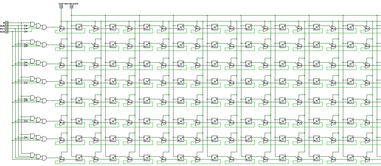
Any suggestions how I can build a RAM8? I guess in a sense it is right but it is not what is required for the software. I'm trying to build up a visual picture for myself to remember what I am making. I've gotten pretty far but am a little stumped here. Also. Doesn't all the bits need to be connected to the master clock?
Reply | Threaded
Open this post in threaded view
|

Re: ABOUT RAM

WBahn
Administrator
Again, don't try to build a RAM8 using 128 individual bits.

Build and test a single 16-bit register.

If you can't understand the concepts well enough to get a single 16-bit register working properly, there is pretty much no hope of getting anything more complicated to work. But once you do understand the concepts of how to get a single 16-bit register to work and pass the tests, then you will be in a good position to take the minor step needed to combine eight of them into a RAM8 (or, to take it in even smaller steps, build a RAM2 using two Register parts, though you won't have a test script for it).

As for the clock signal, yes, every DFF is connected to the same clock. In the simulator this is done implicitly and that's why there's no need to wire it up explicitly in your HDL files.