CPU – second tick – DRegister output

classic Classic list List threaded Threaded
5 messages Options
Reply | Threaded
Open this post in threaded view
|

CPU – second tick – DRegister output

gs99
This post was updated on .
The CPU chip demonstrates the operation of Combinational and Sequential chips. It’s important to know the difference.

In CPU, there are three chips that include sequential operation: ARegister, DRegister, and PC. We’re encouraged to use the built-in versions. “These chips have exactly the same functionality of the Register chip specified in chapter 3, plus GUI side effects.” (page 100) All the other chips are Combinational.

...

[Incorrect technical details deleted by admin. See next two posts. --Mark]

...

I must say this is disappointing, when I’m trying to learn how CPU works with combinational and sequential processing.
• The chip specification comments have an incorrect definition of inM.
• There is a “testing artifact” (failure) when D is modified with D and M destinations.
• A, D, and PC GUI elements are wrong half the time.
• Out file DRegister.out data agrees with the cmp file, so there is no “comparison failure”. But both disagree with actual DRegister.out. And they both disagree with chip Register operation.
It’s hard enough trying to resolve “comparison failures” due to my wrong chip designs. But having these problems in the tools is an unexpected challenge.    

I’ve found similar questions in the forum from previous times. Why not have a “sticky” post that explains all of the problems upfront?
Reply | Threaded
Open this post in threaded view
|

Re: CPU – second tick – DRegister output

cadet1620
Administrator
This post was updated on .
Here is a simple HDL and test script to show what happens and when.

Counter.hdl
CHIP Counter {
PARTS:
    ARegister(in=regIn, load=true, out=regOut);
    Inc16(in=regOut, out=regIn);
}
Counter.tst
load Counter.hdl,
output-file Counter.out,
output-list time%S0.4.0 ARegister[]%D4.3.4 regOut%D2.3.2 regIn%D2.3.2;
output;
repeat 4 {tick, output, tock, output;}
Counter.out
|time|ARegister[]|regOut | regIn |
|0   |      0    |    0  |    1  |
|0+  |      1    |    0  |    1  |
|1   |      1    |    1  |    2  |
|1+  |      2    |    1  |    2  |
|2   |      2    |    2  |    3  |
|2+  |      3    |    2  |    3  |
|3   |      3    |    3  |    4  |
|3+  |      4    |    3  |    4  |
|4   |      4    |    4  |    5  |
At time 0 the register's stored value is 0 and signal propagation through the combinatorial logic has been simulated.
The incrementer's output, which is the register's input, is 1.

TICK -- the register updates its stored value, but no propagation is simulated.
It is now time 0+.  The simulator output shows the new stored value of the register and the old values of all
wires and pins. 'regOut' is a wire so its value is different than ARegister[] which is the register's stored state.

TOCK -- signal propagation is simulated: Aregister[] -> regOut -> Inc16 -> regIn.
The simulator output shows the stored value of the register (which hasn't changed) and the new values of the wires and pins.

Note that the state displayed at times T+ is an artificial state that does not exist in real hardware. Real hardware propagates
its signals as soon as the the stored state changes. Real hardware does not do anything with tock; the signals have finished
propagating long before tock occurs.

See next post for timing information from a real hardware implementation of this counter.

--Mark
Reply | Threaded
Open this post in threaded view
|

Re: CPU – second tick – DRegister output

cadet1620
Administrator
This post was updated on .
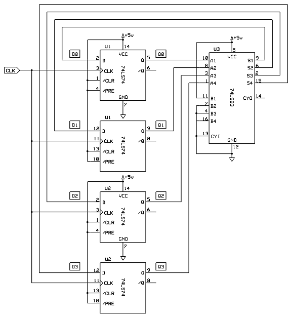
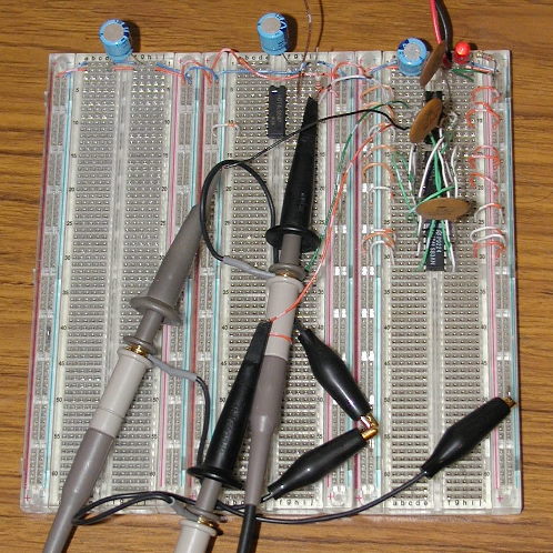
I built a 4-bit version of Counter.hdl using 74LS74 flip-flops and a 74LS83 adder to be able to demonstrate the timing of real world synchronous sequential logic. 74LS74s are positive edge-triggered DFFs. The adder is wired as an incrementer.

This first oscilloscope trace show the clock on the top trace, with bits 0, 1 and 2 on the lower traces. Horizontal scale is 20 milliseconds per major tick mark. Vertical scale is 5 volts per major tick mark. The clock is running at 60 hertz, so the clock period is 16.7 milliseconds.

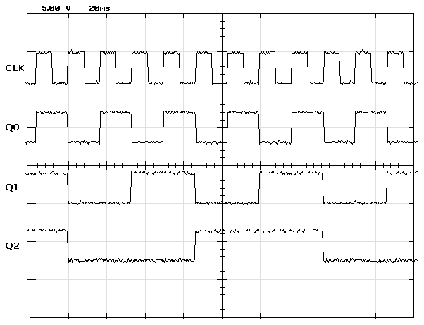
You can see that all the flip-flop outputs change with the leading edge of the clock (tick in Nand2Tetris nomenclature).

So, when do the D inputs to the flip-flops change?


This next trace shows, from top to bottom, the clock, flip-flop output Q0 and flip-flop input D0. Same horizontal scale as the first trace.

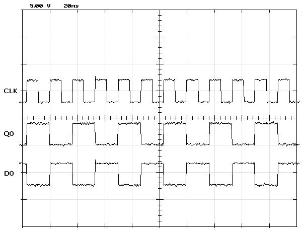
The input, D0, is the output of the incrementer. When a number is incremented, its least significant bit is always complimented. This trace shows that the incremented value of the DFF output appears on the DFF input at the same time as the leading edge of the clock.

Absolutely nothing happens in this circuit at the falling edge of the clock (tock in Nand2Tetris nomenclature).

To see when the DFF input changes relative to the clock and DFF output, we must zoom in on the time scale 1,000,000 times.


This shows the detail of what happens when the clock ticks. From top to bottom, clock, Q0, D0. The horizontal scale is now 20 nanoseconds per major tick mark. (To appreciate how fast this is, light travels 6 meters in 20ns.)

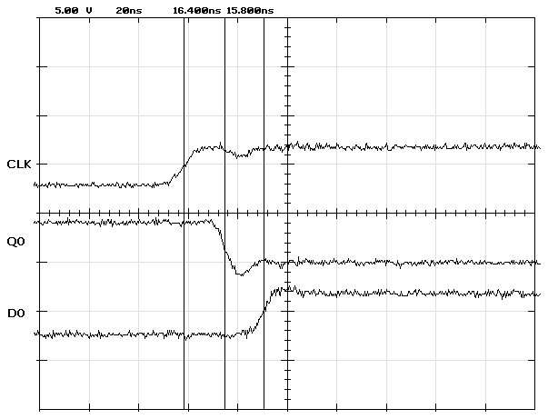
The first thing to notice is that there is no such thing as instantaneous in hardware. It takes a significant amount of time for the signals to change from 0v to 5v (this is called rise time). Timing measurements are usually made from the midpoints of the rise time interval. The DFF output changes 16.4 nanoseconds after the clock. The adder only takes 15.8 nanoseconds after Q0 changes to output the incremented value.

32.2 nanoseconds after the clock tick, signal propagation is complete and nothing will change until the next clock tick.


This final trace shows that there is no such thing as simultaneous in hardware. For this trace we have zoomed in a bit more. The time scale is now 10 nanoseconds per major tick mark. Signals from top to bottom are clock, Q0 and Q2.

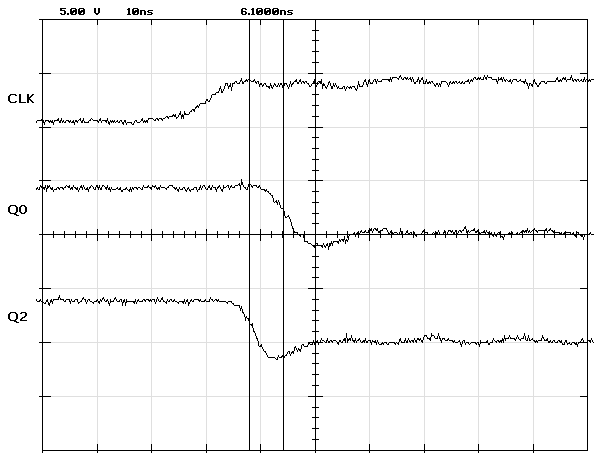
There is a 6.1 nanosecond difference between when Q0 and Q2 change, even though they are controlled by the same clock.

In this circuit Q0 and Q2 are handled by two different ICs, U1 and U2, respectively. U1 is quite a bit slower than U2. Datasheets for ICs only specify the longest time they will take to perform their operation. Nothing is said about how fast the might be. (I did cheat a bit here by intentionally choosing one of the slowest and one of the fastest 74LS74s from my parts box; I wanted a good skew demonstration.)


This is just the tip of the hardware iceberg. I hope you've found this interesting and educational.

--Mark

Reply | Threaded
Open this post in threaded view
|

Re: CPU – second tick – DRegister output

gs99
Thanks for that information.

Everybody learns in different ways; it's beneficial to see other viewpoints.

But I've made progress on this complicated CPU project.

thanks for all the comments.
Reply | Threaded
Open this post in threaded view
|

Re: CPU – second tick – DRegister output

pdudj
In reply to this post by cadet1620
Hello awesome people,

I also got a problem with the script CPU.tst regarding the value of register D on 1+ (tick).

I don't agree with gs99 that it's disappointing : that was the price of not listening to advice !
I didn't pay attention to the advice in the book p100 to use the build-in ARegister and DRegister, and used my own build register from a preceding chapter (and also fiddled with the header of CPU.cmp).

But anyway, understanding our errors allows us to learn ... ;-)

I DO agree with gs99 that the value of D is suspicious (wrong?) on time 1+ (tick).

As (very well) explained by cadet1620 (thank you!), there is no instantaneous propagation on real hardware. As the tick goes, the propagation of the signals start. Nobody knows at what time exactly all the signals will complete their path. BUT as the tock goes, we know that the work is done and that nothing is going to change before another tick. SO IMHO, in the simulation, D register shouldn't change on 1+ (tick) and should be set to ********* (undefined).

As a sidenote, i've successfully run the script CPU-extern.tst without any change to my CPU.hdl file.
It's an evidence that all in/out signals are corresponding to the awaited results of the architecture.

Have fun !

pdudj