Data flip flop has only one input and output??

classic Classic list List threaded Threaded
4 messages Options
Reply | Threaded
Open this post in threaded view
|

Data flip flop has only one input and output??

tyler1313
I'm trying to build the hack computer on a program called logisim. However, in order to build the bit, and then the register, I have to deal with the D Flip Flop, which is a built in chip in the Hack computer so I can't use the file from here to build it from And, Nand, Or, Not, etc gates. When I look up D Flip Flop to see how to build it, it has 2 outputs and 2 inputs everywhere I can find this chip explained. However, the built in chip we use in this course only has one input and one output. My question is why is this the case? (Why does the built in DFF chip have only one input and output)? If this is not a mistake, how do I build the DFF chip with only one input and output?
Reply | Threaded
Open this post in threaded view
|

Re: Data flip flop has only one input and output??

cadet1620
Administrator
The two inputs you see are D and CLK. The nand2tetris DFF (and other synchronous parts) show the clock input as a triangle on the bottom of the schematic symbol, but do not have CLK as an input that you can connect to. The clock is permanently connected to the simulator's system clock so that all synchronous chips in HDL tick and tock at the same time.

The Q output is n2t's "out". the Q-bar output is the inverted value of Q. It can be important in real world hardware design to have the complementary output that change very nearly simultaneously. The extra delay cause by creating the inverted value using a Not gate can sometimes be a problem.  In the theoretical world that is n2t, there is no time delay involved in Not so this is never a problem.

Your Logisim DFF will want to look like this. Having the clk input facing North will place it by default on the bottom of the chip outline.

If you want to make the chip outline look like the n2t drawings, click the circuit outline button on the right end of the second row of buttons, and make the outline look like this.

(Zoom in to 400% to be able to easily make the small lines for the clock triangle.)

Bit's CLK input will want to be north-facing so that it will be on the bottom of Bit's outline.


If you want to learn about the internals of DFF, check out http://www.play-hookey.com/digital/sequential/

--Mark
Reply | Threaded
Open this post in threaded view
|

Re: Data flip flop has only one input and output??

tyler1313
When you say, "The clock is permanently connected to the simulator's system clock" and "all synchronous chips in HDL tick and tock", what is the system clock exactly and what does it mean to tick and tock? I have read chapters 1-6 and can not find the answer to this so sorry if I am asking a stupid question.
Is it just one wire that is connected to every single register in memory that is either a 1 or 0 at any given time? If so, what is that wire connected to? (what is the input coming from) I don't think that could be the case though because wouldn't that set every register to the 16 bit input value of the memory when the "system clock" changes to a 0?
As I understand currently, when the system clock changes to 0, this makes the register value equal to the input value (the input of the register), and when the clock is set to 1, this makes the register value the previous input value. While the clock is set to 1, the input value can change but the register value will remain the same (t-1). Have I misunderstood anything about this?
Reply | Threaded
Open this post in threaded view
|

Re: Data flip flop has only one input and output??

cadet1620
Administrator
tyler1313 wrote
When you say, "The clock is permanently connected to the simulator's system clock" and "all synchronous chips in HDL tick and tock", what is the system clock exactly and what does it mean to tick and tock?
The system clock is the "master clock" that makes sure that all the synchronous parts in the computer update (store their data and present new output values) at the same time.  Physically the master clock is usually a crystal oscillator which is an electronic circuit that provides a periodic signal that has very stable frequency.

See 3.1 "Clock" for tick and tock; basically it means the clock changed from 0 to 1 or 1 to 0.
Is it just one wire that is connected to every single register in memory that is either a 1 or 0 at any given time? If so, what is that wire connected to? (what is the input coming from) I don't think that could be the case though because wouldn't that set every register to the 16 bit input value of the memory when the "system clock" changes to a 0?
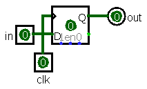
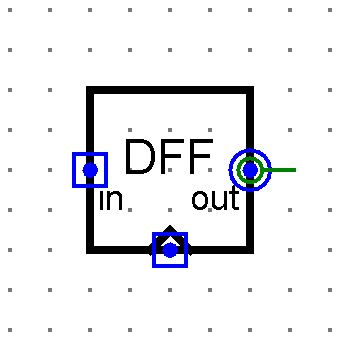
The Registers are made from Bits that only load when their "load" input is true and the clock changes from 1 to 0.
As I understand currently, when the system clock changes to 0, this makes the register value equal to the input value (the input of the register), and when the clock is set to 1, this makes the register value the previous input value. While the clock is set to 1, the input value can change but the register value will remain the same (t-1). Have I misunderstood anything about this?
Master/Slave DFFs are tricky. Experiment with this one
    http://www.play-hookey.com/digital/sequential/d_nand_flip-flop.html
The left 4 Nands are the Master Latch; the right 4 are the Slave Latch.

While CLK is 0, the D input is ignored. If you change it, the Master does not change its outputs.
While CLK is 0, the Slave tracks the output of the Master, but because the output of the Master can not change, the Slave does not change.
When CLK goes 0->1, the Slave is disabled so it no longer is tracking the Master.
While CLK is 1, the Master tracks the D input, and because the Slave is disabled, it does not change.
When CLK goes 1->0, the Slave loads the output of the Master and simultaneously the Master is disabled.

--Mark