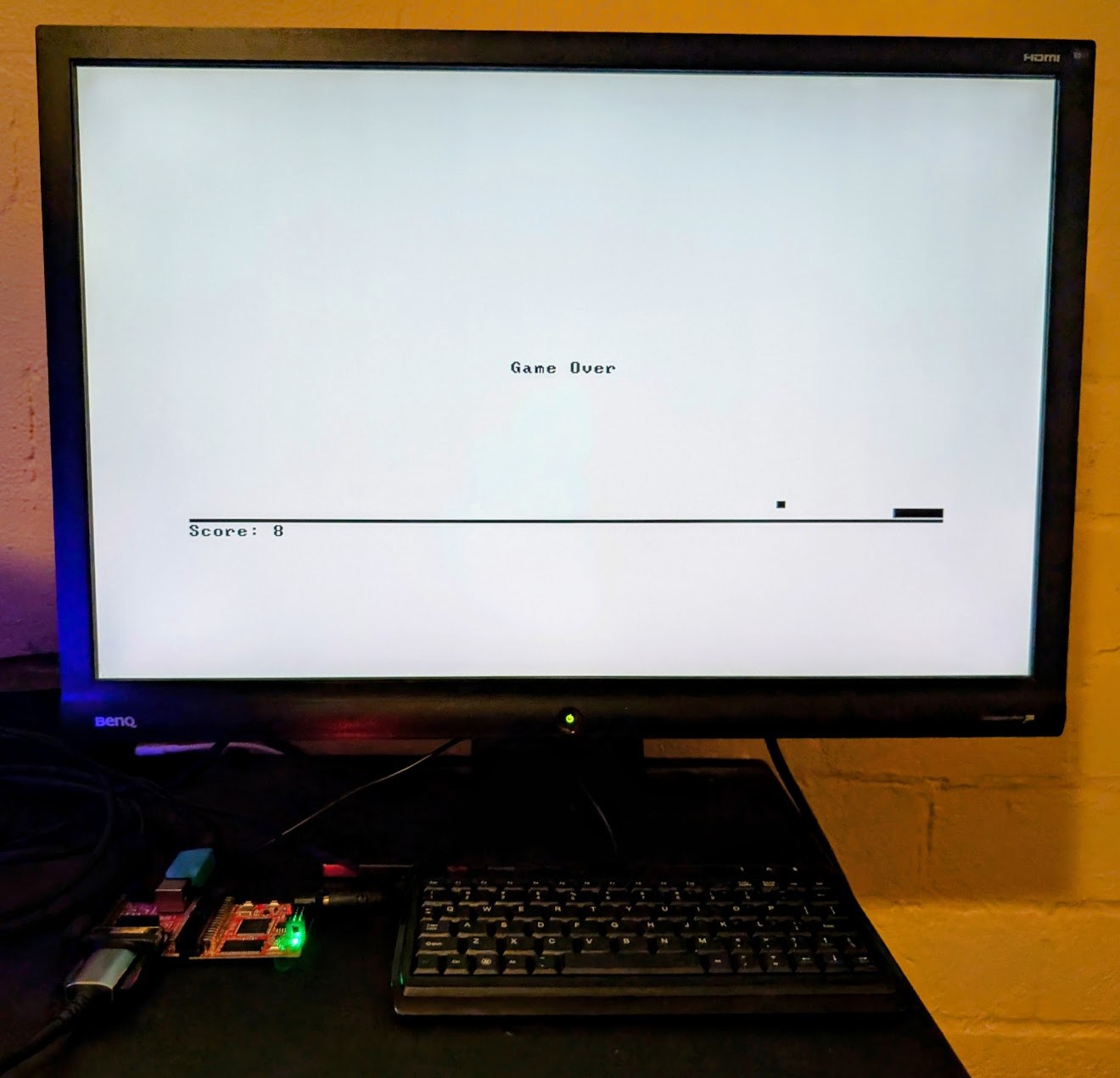
Once again taking inspiration from Michael Schröder, I decided I wanted to build something more faithful to the original nand2tetris spec which means adding VGA and PS/2 support via iCE40-IO and dropping MOD-LCD2.8RTP.
This ended up being not too bad to add the controllers (using his implementation for those, thanks Michael) but it required a really complex series of architectural updates to essentially pipeline all the different accesses to SRAM which unfortunately does not support dual port access. Without any way to parallelize those accesses I had to drop the clock speed as well from 25 MHz to 6.25 MHz just so there was enough time in each "cycle" (which is now several sub-phases but for the sake of nand2tetris semantics some things had to be maintained) for all the RAM accesses to complete (fetch instruction, read VRAM, read/write SRAM).
After these updates I was more or less able to plug in all my original Jack libraries with minimal changes, currently only needs to remap some of the previous memory mapped I/O devices and full ABI & API compatibility will be restored.
I'm happy with the result but a lot of this pain could have simply been abstracted away with a more capable board and perhaps I was being a bit stubborn there.
https://github.com/c0ff33-dev/nand2tetris-fpga/tree/main/09_More_Fun_to_Go