[There have been some recent questions about race glitches and propagation delay on the Coursera forum, and I remembered that I had a nice timing digram somewhere on my work computer...]
A while ago, as part of a Verilog refresher (I was going to need to add some functionality to an FPGA in one of my customers' products), I wrote a Verilog implementation of the Hack Computer using the suggested design hierarchy and the most common student designs for the parts. I also implemented DFF in Nands, using the classic cascaded SR-latch design.
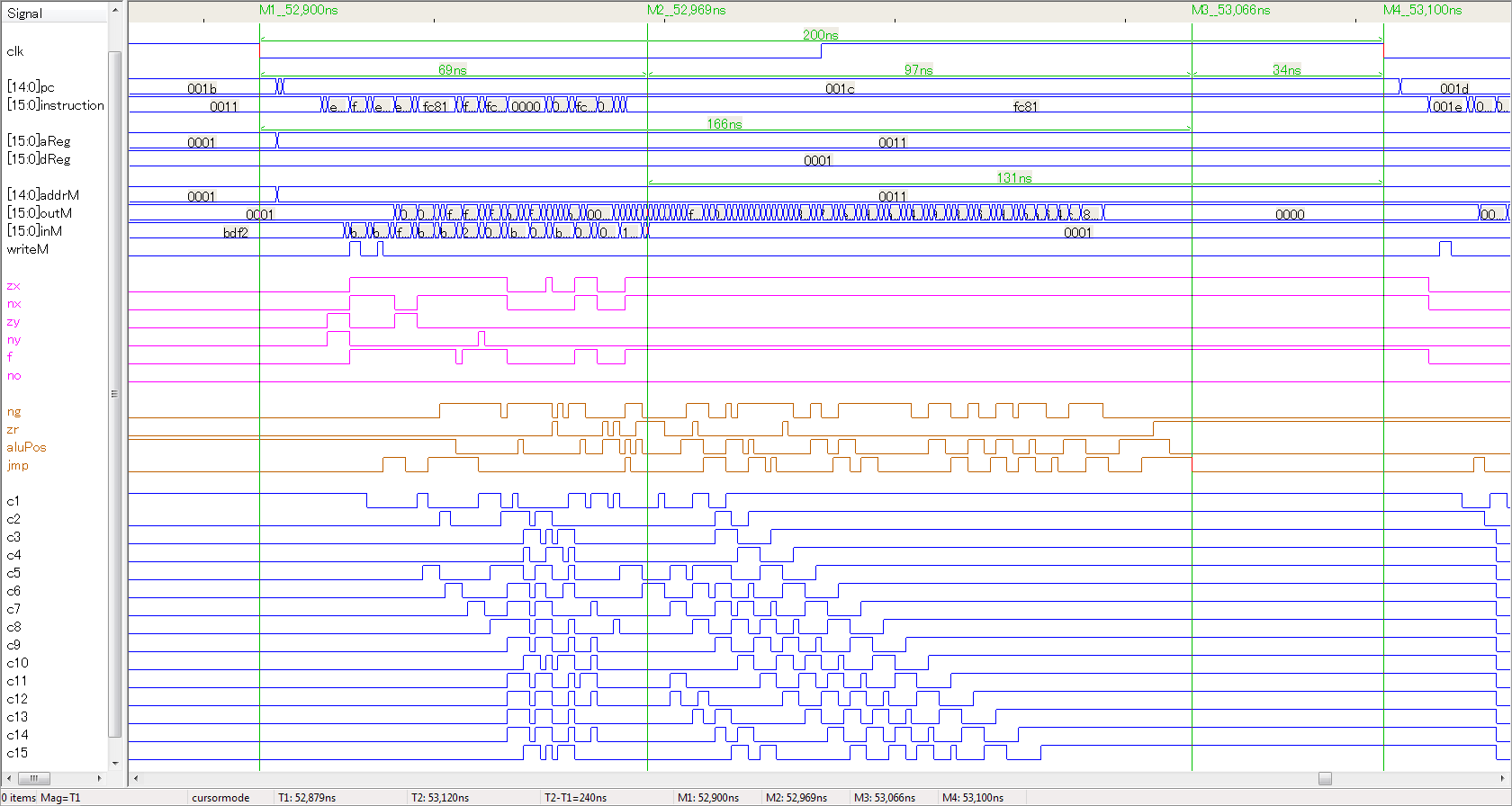
Here's a timing diagram from that computer. It shows how messy the signals can get when propagation delay is added into the simulation.
This is a trace showing the execution of one instruction. The simulated Nand gate delay is 1 nanosecond (ns).
The instruction being executed is M−1;JGT, with the data value 0x0001 being read from memory. This is a bit of a nonsense instruction, but it exhibits maximum computation and jump detection delay.
The upper blue traces are the Computer's inputs, outputs and Registers.
The pink traces are the command inputs to the ALU.
The brown traces are the ALU status outputs, the "pos" status computed from the status outputs, and the jump control signal (PC load).
The lower blue traces are the ripple-carry signals in Add16.
What's Happening When
|
M1 |
t=0 | The clock triggers, executing the previous instruction which was @11. |
|
t+5 | A Register1 and PC finish updating; ROM and RAM addresses are stable. |
|
t+11 | The "instruction" and "inM" both have the potential to start glitching here. "InM" did not do so in this simulation due to RAM contents being mostly zero. (The highest address bits are connected to the muxes closest to the output, and they are selecting between memory cells that all held 0.) |
|
t+12 | The ROM's address select multiplexor glitches propagate immediately to the ALU command input because it is wired directly to "instruction". |
|
t+19 | The ALU is feeding random values to the Add16 because of the strange command codes and "inM" values. There is lots of random carries rippling up the full adder chain. ALU output ("outM") and status and jump control signal are chaotic. |
|
M2 |
t+69 | "instruction", "inM" and the ALU command have settled, but the correct input data needs to propagate through the zero and not mutiplexors to get to the Add16. |
|
t+83 | The data has finally arrived at the Add16 so it can compute 1 + −1. You can see this computation happening as the full adder chain generates the 15 carry bits for this addition. |
|
t+139 | The ripple-carry has arrived at bit 15 |
|
t+150 | ALU "ng" status settles to false, indicating that the carry has propagated through the bit 15 full adder and the ALU's output multiplexor.2 |
|
t+159 | ALU output bit 15 has propagated through the zero-detect circuit.3 |
|
M3 |
t+166 | All of the combinational logic for the instruction has settled. |
|
M4 |
t+200 | The clock trigers, storing new (if required by the instruction) values into A, D and M and incrementing or loading the PC. The next instruction begins decoding. |
|
| 1
The reason the PC glitched and the A Register did not is that the only bits in the A Register that changed went from 0 to 1. The classical Nand DFF is one gate delay slower going from 1 to 0. 00011011→00011111→00011100
|
| 2
The long delay while the carry propagates through the ripple-carry adder is why more complex adders like the Carry Look-ahead Adder are used in most real systems.
|
| 3
The delay from ALU out[15] to ALU zr points out that this is a critical path; if the delay can be reduced the CPU can run faster. Or8Way is a binary tree of Or gates so that it has equal delay for all its inputs. In this usage, immediately following the ripple-carry adder, chained Or gates would result in bit 15 having a single Or delay instead of 4 Or delays. The delay through the earlier Ors in the chain would be happening in parallel with the carry delay through the adder.
|
How Fast Can the Computer Run?
It appears that the clock for the next instruction could occur any time after the logic settles; as soon as t+167 which would yield a maximum clock speed of 5.98 Mhz. However, there are some things that need to be taken into consideration.
The first thing is the setup time for the DFFs. Setup time is how long the inputs must be held valid before the clock triggers. For the Master-Slave DFFs this is 2 Nand delays. In the real world, random extra delays like the lengths of interconnecting wires mean that we can not design for exactly 2ns setup time; the clock should be at least 3ns after the logic settles.
More important is that the simulation can not be assumed to be an accurate reflection of the real world. There may be bugs in the design of some of the simulated parts (It is not possible to simulate the RAM and ROM to the Nand gate level because there would be about 4.5 million in the RAM.) And there may be data patterns that were not considered that cause slightly longer delay.
Also, beyond what the simulation tells us, we need to consider how much variance there is in the manufacturing process for the parts used to build the computer. The delay times may vary noticeably from lot to lot. The manufacturer's specs will tell us what to expect.
Designers need to include a safety margin beyond the calculated worst case timing to handle unexpected changes during production. In this timing diagram, the margin is (34−3)/200, about 15%. (200ns was a convenient round number.)