|
|
|
|
I'm considering the idea of using a special kind of XOR based entirely on NAND, but which provides two outputs: the usual XOR output and a special output which is the inverted carry. This could be used to then form a half adder and full adder.
The NAND structure is the usual one for XOR, using four NANDs:
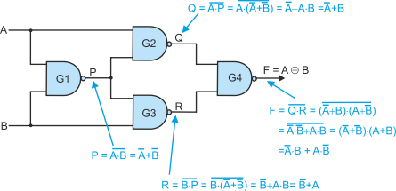 In this case, I'd like to also output the "P" value output of G1 shown in the diagram as the NCARRY (or negated carry bit.)
The trouble I'm having is in wiring up P to the chip output AND also wiring it into the inputs of G2 and G3. I'm getting an error even though there is no unstable loop formed by the use of an output chip pin as inputs to G2 and G3 (which then drive G4.)
How can I achieve something like this:
CHIP XorS {
IN a, b;
OUT sum, ncarry;
PARTS:
Nand( a=a, b=b, out=ncarry );
Nand( a=a, b=ncarry, out=q );
Nand( a=ncarry, b=b, out=r );
Nand( a=q, b=r, out=sum );
}
I get an error with the above. Is there a way to specify an internal "wire" that I can then "tie" to ncarry? Something like:
CHIP XorS {
IN a, b;
OUT sum, ncarry;
PARTS:
Nand( a=a, b=b, out=p );
Nand( a=a, b=p, out=q );
Nand( a=p, b=b, out=r );
Nand( a=q, b=r, out=sum );
ncarry=p;
}
I'm just stuck on this one for now.
Thanks in advance,
Jon
|
|
|
Oh, cripes. I just found out how. I do this:
  CHIP XorS {
    IN a, b;
    OUT sum, ncarry;

    PARTS:
    Nand( a=a, b=b, out=p, out=ncarry );
    Nand( a=a, b=p, out=q );
    Nand( a=p, b=b, out=r );
    Nand( a=q, b=r, out=sum );
  }
  CHIP HalfAdder {
    IN a, b;
    OUT sum, carry;

    PARTS:
    XorS( a=a, b=b, sum=sum, ncarry=nc );
    Nand( a=nc, b=true, out=carry );
  }
  CHIP FullAdder {
    IN a, b, c;
    OUT sum, carry;

    PARTS:
    XorS( a=a, b=b, sum=sumab, ncarry=nc1 );
    XorS( a=sumab, b=c, sum=sum, ncarry=nc2 );
    Nand( a=nc1, b=nc2, out=carry );
  }
I just needed to read the survival guide better. Tricky!
Jon
|
|
Administrator
|
Here's an experiment for you:
Create a Nor chip.
Use 4 of them in the same circuit topology as your XorS.
What function do you get?
Use 9 Nor chips in the same circuit topology as your 9-Nand full adder.
What function do you get?
I love this type of magic—quite aesthetic.
--Mark
|
|
|
This post was updated on .
Well, let me start with the reasoning behind the XOR's NAND-only structure where I'm only permitted NANDs to make an XOR, where XOR = (A)~(B) + ~(A)(B):
1)     XOR(A,B) = NAND(P,Q) = ~(P Q) = (~P) + (~Q) = (~A)(B) + (A)(~B)
2)     therefore, ~P = (~A)(B) and also ~Q = (A)(~B)
3)     but,
            ~P = (~A)(B) + (~B)(B) = (B)[(~A) + (~B)], and also
            ~Q = (A)(~B) + (A)(~A) = (A)[(~A) + (~B)]
4)     since (~A) + (~B) = NAND(A,B), things get real easy.

        XOR(A,B) = NAND(NAND(B,NAND(A,B)),NAND(A,NAND(A,B)))
So only four NANDs are required.
The above logic required the addition of (A)(~A) in one case and (B)(~B) in the other in order to "discover" the simplifying approach. This doesn't fall out of the usual K-map or Quine-McCluskey methods, both of which equally suggest using five NAND gates. It simply takes creativity, it seems, to apply (A)(~A) and (B)(~B) in order to "find" a possible simplification using NAND gates.
If you know of any software which will automatically find this, let me know. I haven't seen any yet.The other wonderful aspect of this is, unlike the more obvious case where five NANDs are used with two of them as inverters, the NAND(A,B) output also works nicely as a NOT CARRY value. So a single XOR provides both a SUM and a NOT CARRY output, while at the same time using four gates instead of five.
Nice.
Now to the NOR case. Using four in the same topology I get:
  F = ~(~[B + ~(A + B)] + ~[A + ~(A + B)])
  F = [B + ~(A + B)] [A + ~(A + B)]
  F = [B + (~A)(~B)] [A + (~A)(~B)]
  F = (A)(B) + (~A)(~B)(A) + (~A)(~B)(B) + (~A)(~B)(~A)(~B)
  F = (A)(B) + (~A)(~B)
So the output is as if I had F = XNOR(A,B).
Too bad I don't have any NOR gates since this is a NAND class!
For all nine gates as NORs, I get the same output -- a full adder!
Jon
|
|
Administrator
|
cadet1620 wrote
Use 9 Nor chips in the same circuit topology as your 9-Nand full adder.
jonk wrote
For all nine gates as NORs, I get the same output -- a full adder!
Nor gates, like Nand gates are universal primitives. There was a family of ICs in the 60's and early 70's called ECL whose natural gate was Nor. It was very fast but also power hungry.
De Morgan's law for Nand says
Nand( a, b ) = Not( Nand( Not(a), Not(b) ) )
The normal canonical design and optimization tools like Karnaugh maps all work backwards. You need to consider inverted input and output values. This makes designing with Nors harder than with Nands—it helps if you brain is abNORmally wired.
This 9 gate design for full adder has always been one of my favorites because it is identical with either Nand or Nor gates.
Too bad it is too slow (6 gate delays) that it is not used in practical hardware designs.
--Mark
|
|
|
This post was updated on .
I've used ECL only the early 1980's. They keep the BJTs out of saturation for speed. Nice.
My experience in designing CPUs is mostly where I've targeted Xilinx FPGAs (4000 series, back in the day) using VHDL. I only have very limited experience with verilog.
Carry look ahead, of some form, is usually used with adders. I understand that. Usually where some kind of balance is struck between group size, acceleration of carry, propagation delays, etc. Non-trivial, in practice. But fun.
In the case of the 9-NAND full adder, and assuming NAND as the canonical delay, the carry out takes 5 gate delays and the sum takes 6 gate delays. One less gate delay is only a small bit of luck, though. As you add stages, this gets to be pretty ornery, of course, as the carry ripples across stages.
By the way, I've not yet gotten far enough into the course. But subtraction is really quite easy without a new function code for the ALU. You can mux the Q and /Q outputs from registers to select the complement and then feed (mux) in a "1" as the carry into the ALU in order to complete the twos-complement negation and create a subtraction. Even when the ALU itself only supports addition directly. Just a matter of execution control logic, is all.
I'm really enjoying the simulator that accepts a modest HDL language. I would like to consider doing more with it -- including allowing folks to enter combinatorial and sequential logic using schematic capture, logic tables, and so on. Perhaps more. I guess I wish there were a very nice, very flexible tool that was freely available and where people can use whatever they prefer in terms of describing each aspect of their project. I'd also like it to be capable of accepting constraints and doing an excellent job of optimizing (say, a table) to a set of logic and/or selected chip specifications. That part seems the most interesting to me -- and difficult. But fun.
Thanks so much for discussing this and suggesting taking a quick look at the NOR, as well. It's been decades for me since I'd bothered much with this stuff and the interaction really helps me a lot to recover and re-think stuff I've long since forgotten now.
I'm also VERY glad to see someone, anyone really, trying to invigorate an interest in how computers work. One of the only books I know of, perhaps aside from the one recommended for this class, is "Bebob BYTES Back: An Unconventional Guide to Computers" by Clive Maxfield and Alvin Brown. That is, one that is targeted at someone completely untrained in this area.
I built my first computer at home using 7400 series gates and a HUGE amount of wire-wrap. I also designed the power supply for it. This was in 1974. It was a wonderful experience.
I'm considering the idea of developing a series of physical modules, something akin to Elenco's 750R kit of Snap Electronics. I'd like to base it on a 4-bit bus width per "connection" so that an 8-bit ALU isn't trivial and requires "some work" while at the same time not having to have an entire floor available for laying out a full CPU. I think slicing it at 4 bits might force enough learning while at the same time making a full 8-bit CPU achievable without near-infinite floor space to complete it. With the availability of micros at such cheap cost, it shouldn't have to be too expensive. I've already contacted Elenco about the possibility of having them manufacture the plastic modules with conductive connections and they've responded positively about the idea and are willing to help out. So it may yet happen. Just depends on what I can do, given other distractions in life.
Just as a by-the-way, I spent some 1:1 time with Dr. Hennessey at MIPS, back in 1985/1986 time-frame, when working on the R2000 RISC processor (actually a small collection of chips.)
|
|
Administrator
|
Great to see another old-timer on the forum.
Feel free to jump in (please!) and answer people's questions from your experience.
There's another book by Maxfield and Brown, "How Computers do Math", that you might find interesting.
http://www.clivemaxfield.com/diycalculator/(I haven't seen Bebop Bytes Back yet, should be in my mailbox any day now...)
Carry look ahead, of some form, is usually used with adders. I understand that. Usually where some kind of balance is struck between group size, acceleration of carry, propagation delays, etc. Non-trivial, in practice. But fun.
There are some forum threads on various adder designs
About carry lookahead adder Carry Lookahead Implementation Carry Select Adder (includes Carry Bypass Adder)
--Mark
|
|
|
This post was updated on .
Hehe. I really LOVE this whole process. (Did chipset testing, which also involved lots of FPGA programming, for Intel circa the BX chipset and the Pentium Pro and Pentium II days. And worked on CPU emulation using a huge box literally FILLED with Xilinx FPGAs all eventually hooked up to a tiny little CPU socket connector!)
For those interested in learning, from scratch, about both VHDL and verilog and who may also like to see side-by-side comparisons, as well as some interesting and very useful implementations that may be useful in moving towards a CPU design, I also enjoyed Mr. Smith's "Hdl Chip Design: A Practical Guide for Designing, Synthesizing & Simulating Asics & Fpgas Using Vhdl or Verilog" book. He came to the US from Britain and settled first in Alabama, I think. (I had occasion to talk with him on the phone for a while when he first arrived here in the US late in the 1990's.) It is very handy to see the left page showing something in VHDL and the right page showing the same something done up in verilog. And the book is for newbies. So very nice in that regard.
I also like and have these:
"Microprocessor Design Using Verilog HDL" by Monte Dalrymple.
"VHDL: A Starter's Guide, 2nd edition" by Sudhakar Yalamanchili
"RTL Hardware Design Using VHDL: Coding for Efficiency, Portability, and Scalability" by Pong P. Chu.
They are all good, I think.
Thanks so much for the links to some interesting, additional threads to look over.
Jon
P.S. I really DO wish the simulator had included a nice "for" to help reduce the number of lines I have to type in. Oh, well.
|
|
|
This post was updated on .
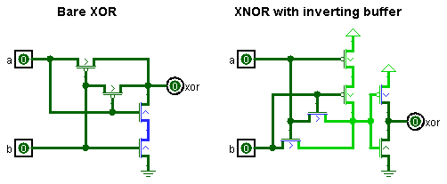
By the way, I think I recall that in CMOS the NAND is preferred to the NOR, as the propagation delay is significantly shorter for the NAND structure (two N-channel devices in series to ground for NAND vs two slower P-channel devices in series to the Vcc rail for NOR.) But the 4-NAND XOR would require some 16 transistors.
Faster XOR circuits don't depend on NAND. They just use A as a MUX selector for transmission gates passing along B and /B to the output.
|
|
Administrator
|
CMOS does prefer Nand over Nor. INACD *, but my reading says that the issue is one of transistor size. Because holes have about 1/3 the motility of electrons, PMOS transistors need to be 3 times the width to have the same on resistance as their matching NMOS transistors.
Given 1 as the smallest size, then the Not gate will have a 1-sized pull-down and a 3-sized pull-up.
A Nand will have 2 3-sized pull-ups in parallel and 2 2-sized pull-downs in series for total size 10.
A Nor will have 2 1-sized pull-downs in parallel and 2 6-sized pull-ups in series for a total size of 14.
The ratio gets worse as the number of inputs goes up.
For the transmission gate Xor you need both A and /A as well as B and /B. There are some tricky Xors that use pass transistors that can be used internally in a chip, but need to be buffered with a Not if you need full output drive.
--Mark
* I'm not a CMOS designer. This is all from book learning.
|
|
|
The bare XOR, as you show it, has a few problems. The voltage swing at the output isn't full-swing and it has a very limited driving capability and it doesn't work so well at lower voltage rails. There are some different arrangements with better drive, at the cost of higher power.
Also, XOR _and_ XNOR are often simultaneously needed in compressor cells used in multipliers, for example. So there is a need for something that achieves both at the same time and where there isn't a difference in propagation delays for the two outputs, as well (which would obviously exist if you used an inverter at the output to get the extra signal.)
There's a nice 8-transistor XOR cell which provides good drive and works well with low voltage rails. But the use of two inverters at the input increases its power consumption. And using an inverter also at its ouput adds still more power consumption (plus a largish skew between the XOR and XNOR output attending the addition of the inverter.)
Some interesting arrangements have been used to provide both XOR and XNOR without skew and workable at low Vcc voltages, have high drive capability, and handle high relative noise levels. Additions using dual feedback arrangements are quite noise tolerant and also provide a significant improvement in the power-delay product.
Holes, as you say, have quite a bit lower mobility. I believe I also learned that the ratio is about 3:1, but I think modern devices and doping level differences allow perhaps closer to 2:1, now. If my memory is right about that, the input loading difference between a NAND (parallel P-MOS on top, series N-MOS on bottom) vs a NOR (parallel N-MOS on bottom, series P-MOS on top) is about 4:5. Assuming a straight inverter loads as "3", given a double-sized P-MOS and a single-sized N-MOS both driven by the input, then a NAND input must drive one of a pair of double-sized N-MOS on the bottom (as they are in series) and a usual double-sized P-MOS on top, for a load of "4". And a NOR must used a quad-sized P-MOS on top (as they are in series there) and a single-sized N-MOS on bottom, for a load of "5". Hence the 4:5 comparison between them, input loading wise. (Output drives are the same.) Of course, if it is still 3:1 for P vs N, then the above calculations will be changed appropriately. (Loading is a reasonable analog for propagation delay.)
I never did that much with carry look-ahead. I used the slices available in FPGAs, so it wasn't something I needed to learn more about. I'm still reading through those pages you linked, though. I'd like to fully understand both the mathematics as well as the specific implementations you mentioned. In particular, though, I'm curious about modifying your PFA concept to use the /carry output of a 4-NAND XOR instead of using a separate AND gate to generate the G signal. In short, I'd like to see the logic using a /G output, instead of the G output. I'm going to enjoy playing a little bit.
|
|

