Understanding Clock Cycles

classic Classic list List threaded Threaded
5 messages Options
Reply | Threaded
Open this post in threaded view
|

Understanding Clock Cycles

elshae
I am a student working through the book as an independent study with a professor of mathematical logic. We are trying to understand the clock cycles which are at the heart of the memory gates in chapter 3. We both lack a background in computer engineering and architecture. Below is our abstract analysis of the bit gate and we would like to know whether we are correct:


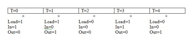
Note: Each clock cycle is an interval and is depicted by a box above, + indicates the tick

In the first run(T=0 @ tick), where we have (Load=1 & In=1), these inputs are not considered yet and out = 0. On T=0 @ tock, out =1 because load & in = 1, T is now equal to 1. When T=1 is @ tick and Load = 1, In=0, Out = 1 (in(T-1)), but when T=1 is @ tock, then the Load=1 and In=0 of T=1 @ tick is considered and Out = 0 and T=2. When T=2 @ tick and Load=0 and In=0, Out is still the same as In(1). When T=2 is @ tock then Out is actually Out(T-1) which is Out(2) because T is now equal to 3, the beginning of the next clock cycle.

Does this mean that when T is at tock, it is updated to T+1 first so that Out can equal Out(T-1) or In(T-1), before the In and Load bits are even considered?

Thanks in advance, your feedback is truly appreciated,

elshae
Reply | Threaded
Open this post in threaded view
|

Re: Understanding Clock Cycles

ybakos
I highly recommend that you read Code (by Petzold), specifically the chapter on Flip Flops. Knowing how the edge-triggered flip flop works as a circuit is much better than resting on its theoretical behavior (in my opinion). Once you see how the circuit works, the whole input(t-1) vs. output thing becomes simple to grasp.

These interactive circuit diagrams also help:

http://www.play-hookey.com/digital/d_nand_latch.html

I'm not sure about your plaintext description of the behavior... to me, it's really summed up by the PC specification (see the 'Function' declaration) and the digram below it, on page 51.
Reply | Threaded
Open this post in threaded view
|

Re: Understanding Clock Cycles

Todun
In reply to this post by elshae
"... output pins stabilize to new values only at tocks...", from appendix a, suggests that the data-flip-flop(DFF) used is a latch. This means that the DFF is level-tiggered and thus the output reflects the inputs(controlled by the load signal in the case of a register) at the high level(tock) but stores during the low level(tick). By design therefore, the DFF retains data at a time that is one period ago, T-1, and makes it available at the current time T. So starting from time T(start of next tick and end of previous tock), out(T)=[ load(T-1) AND in(T-1) ]. At time +T (tick), out(+T)=out(T)=[ load(T-1) AND in(T-1) ]. During T+1(tock), out(T+1)=[ load(+T) AND in(+T) ]. Then at end of tock(+T+1), out(+T+1)=out(T+1)=out(current-time)=[ load(previous-time) AND in(previous-time) ].

Hopefully all this is correct and helpful. Petzold's Code gives an authoritative, but clear, insight to DFFs.
Todun.
Reply | Threaded
Open this post in threaded view
|

Re: Understanding Clock Cycles

ybakos
I disagree.

The DFF in TECS is is an edge-triggered, negative-transition flip-flop.

It's edge triggered because the output is only affected at the very moment of a tock. It's negative transition because the input(t-1) is reflected by output(t) when the voltage moves from 1 to 0 (more or less, there are physical thresholds).

Lastly, while I do like the book "Code" quite a bit, I wouldn't call it "authoritative." There are many small mistakes, and we should all realize that Petzold is trying to be illustrative, not necessarily authoritative.

Reply | Threaded
Open this post in threaded view
|

Re: Understanding Clock Cycles

Todun
Thanks for the update and correction ybakos. I stand corrected. Sorry if I confused you elshae.
Todun.