Re: RAM8 Script test pattern
Posted by cadet1620 on
URL: http://nand2tetris-questions-and-answers-forum.52.s1.nabble.com/RAM8-Script-test-pattern-tp4026159p4026162.html
If you want to learn more about asynchronous circuits including how they are used to built a DFF, check out play-hooky.com. There's a lot of other interesting stuff on that site too.
By input side of the circuit I mean the logic between the chip inputs and the storage elements--the Registers. The output side is the logic between the storage elements and the chip output.
Since the input to the Registers can't be observed directly by the test, the only way to test the input circuitry is by clocking the chip so that the input is transferred (if it should be) to the output. Some aspects of the output circuit can be tested without clocking the chip. In particular, changing the address changes which Register's output should appear on the RAM8's output. That's what the evals are about.
--Mark
URL: http://nand2tetris-questions-and-answers-forum.52.s1.nabble.com/RAM8-Script-test-pattern-tp4026159p4026162.html
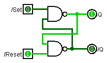
Sorry, I should have said "combinational". You are correct that all the sequential logic in Nand2Tetris is synchronous. Asynchronous sequential logic is when you have feedback but no clocked storage elements like DFFs. Here's an example:
If you want to learn more about asynchronous circuits including how they are used to built a DFF, check out play-hooky.com. There's a lot of other interesting stuff on that site too.
By input side of the circuit I mean the logic between the chip inputs and the storage elements--the Registers. The output side is the logic between the storage elements and the chip output.
Since the input to the Registers can't be observed directly by the test, the only way to test the input circuitry is by clocking the chip so that the input is transferred (if it should be) to the output. Some aspects of the output circuit can be tested without clocking the chip. In particular, changing the address changes which Register's output should appear on the RAM8's output. That's what the evals are about.
This is testing that data gets stored in Register 3.
This is testing that writing to some other Register did not affect Register 1.
Actually, there are greatly more reads from memory than there are writes. During reads, clocking the Registers has no effect; the RAM is acting completely combinationally. Although the Hack computer clocks the memory for every instruction, most real world computers do not. Real world memory systems are extremely complex, well beyond what can be dealt with here.
--Mark
| Free forum by Nabble | Edit this page |