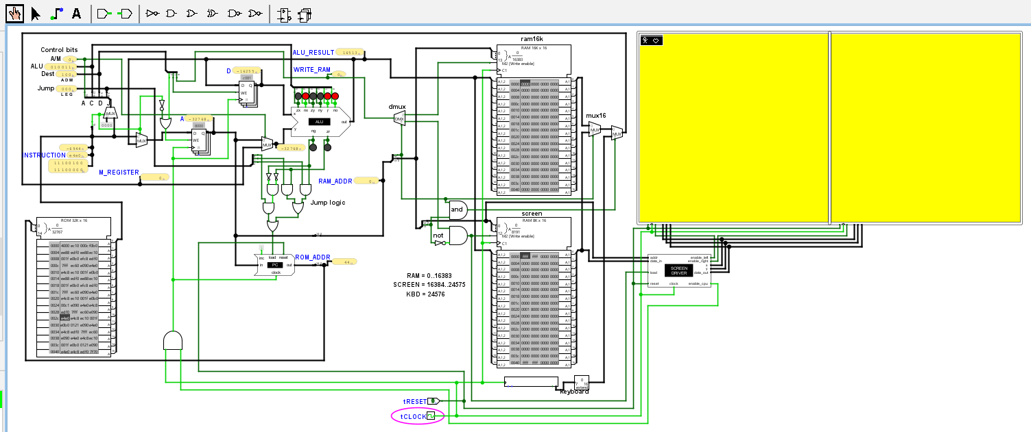
I put together the entire Hack computer in Logisim-evolution. I highly recommend to use the built-in chips (muxers, ROM, RAM, 16bit ADD, etc.). You can build chips hierarchically, but if you build EVERYTHING from NAND gates, Logisim will struggle after some point (mostly because of the ROM).
Still, I recommend to construct all the chips from the smaller (built-in) components!
Also, it's a fun project to make a working screen included. You cannot display the pixels from the RAM directly, as it works with the Hack emulator. Also, the largest screen is 256*256 in logisim. So I put together two such screens and designed a screen driver chip that basically "steals" the clock from the CPU whenever there is a writing into the SCREEN address territory, and for 16 cycles it refreshes the screen bit by bit (pixel by pixel) to the correct screen.
Unfortunately, it is extremely slow.
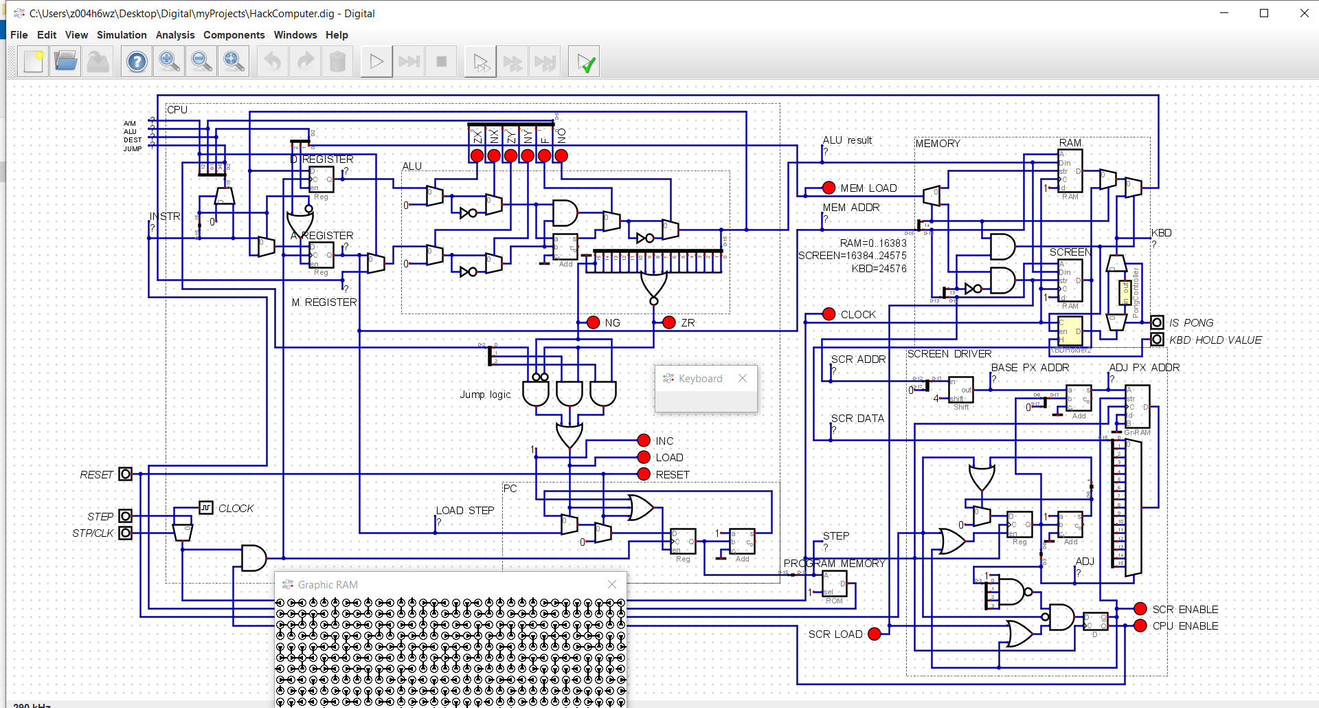
So I did the same thing in Digital. It is much faster, you can play Pong; although I had trouble making a decent Keyboard driver chip.