Hack II: Escaping the Harvard straitjacket

classic Classic list List threaded Threaded
6 messages Options
Reply | Threaded
Open this post in threaded view
|

Hack II: Escaping the Harvard straitjacket

cadet1620
Administrator
A few days ago Andreas asked some questions that made me think about the feasibility of writing a native VM emulator for Hack. The first big problem that occurs is that you can't bind the emulator and the VM code into a .hack binary and load it into the ROM because the emulator can't read data from the ROM.

So I started thinking about ways to upgrade the Hack CPU so that it could programmatically read the Program Memory. I specifically didn't want to go to a two cycle fetch/execute design. Hack is slow enough already. I also wanted to be able to run Hack I programs on the Hack II computer.

What I came up with is to use bit 15 of the A-register to indicate which memory should be accessed. Code addresses will all have bit 15 set, so to access word 0x123 in code memory use address 0x8123. When the CPU detects a memory access instruction and A[15] is set, an extra cycle is inserted to execute the Program Memory access.

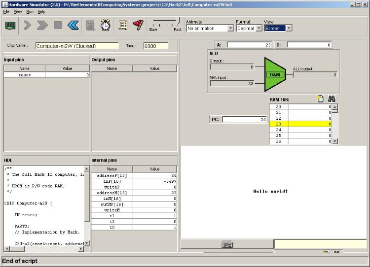
After a couple late evenings I've got Hack II running on the hardware simulator. Now it's time to start writing the documentation. (Like most projects, the hardware's ready but the design docs haven't been completed yet.)

Here's the basic design info. When I get more written I'll post a link to my web page.


The design goals for the Hack II computer are:
  • All valid1 Hack I programs must run on Hack II.
  • There must be a way to read Program Memory into a register.
  • There must be a way to write a register to the Program Memory; it does not need to be ROM.
  • Instructions that do not access data in Program Memory will execute in one clock.
  • No additional instructions are required.
  • A=M;JMP must jump to the newly read value of A.2
1 Valid Hack I programs never attempt to read or write to memory addresses with bit 15 set.
2 This defines a previously undefined behavior, and allows a single instruction jump through a pointer. This might be useful for jump tables.


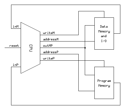
Hack II Computer architecture

Program Memory can be RAM or ROM. If ROM, writes to it are ignored. (Clever programs can determine if they are running in ROM.) Since writes to Data and Program Memory never occur at the same time, they can share a common output bus.

Normal instructions execute in one clock cycle called t1. Instructions that access data in Program Memory require an extra clock cycle called t2. This timing diagram shows how t2 is inserted for the Program Memory accesses, and what data is on the various buses at what time.


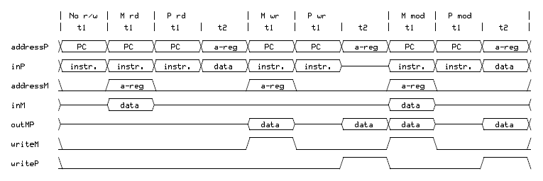
Hack II CPU timing diagram

The instructions shown are: (No r/w) no memory access, (M rd) Data Memory read, (P rd) Program Memory read, (M wr) Data Memory write, (P wr) Program Memory write, (M mod) Data Memory modify and (P mod) Program Memory modify.

When a bus on the timing diagram shows a midline value, the bus's output is undefined or its input value is unused.

addressM is forced to 0 except during Data Memory accesses. The Hack I computer always puts the A-register's value on addressM. On Hack II this could result in inadvertent reads from the Screen and Keyboard when addresses for the upper 16K of Program Memory are present in the A-register. These reads are benign for the current Hack I/O modules, but that may not be the case in the future.


--Mark
Reply | Threaded
Open this post in threaded view
|

Re: Hack II: Escaping the Harvard straitjacket

cadet1620
Administrator
As is normal in software projects, the documentation was more work than the implementation.  The whole project is now on my site.
    http://www.marksmath.com/tecs/hack2
Full source included.

There's even a "hello world" program written in assembly language.  It manages to write "Hello world!" to the screen in less than 5300 clock cycles.  (The OS's Output.vm takes 3.9 million cycles to create the font table in RAM.)

The HW simulator freaks out a bit at data in code and rearranges the screen panel as soon as it loads the code, before running any instructions.

That's enough fun for now.  I think I'll sleep for the rest of the weekend. 8-)

--Mark
Reply | Threaded
Open this post in threaded view
|

Re: Hack II: Escaping the Harvard straitjacket

culchie
Hi Mark
This looks very impressive and interesting.
At some stage (probably after I get around to finishing the compiler and OS!) I'm definitely going to delve into it so get that documentation finished!
Reply | Threaded
Open this post in threaded view
|

Re: Hack II: Escaping the Harvard straitjacket

Raffzahn
In reply to this post by cadet1620
Nice Idea.

But to my understanding not realy a gain nor would it be used that way in an real world application.

For one Addresses now need double calculation, where a in programm reference (like a jump) uses the address x'0010', accessing the same address now would mean calculating x'8010' not intuitive nor easy.

A more natural way to include the Programm Memory (P), would be to add it as another source and destination in the Compute command to access P[A] and make P dual (multi) ported. Especially when we think about an implementation with todays standard hardware (FPGA or on similar blocks based ASIC) , multi ported RAMs (2xRead 1xWrite) are most basic. That way we not only keep the basic HACK structure, but also make it keep it's 1 cycle design.

To controll the P(A) access, an additional bit is taken from the compute Prefix, just left of 'a'. As a matter of fact, 'a' is already kind of a source field, since it defines if A or M[A] is taken as an input to the ALU. With two bits of 'a' we now define:

10 -> A (as HACK I)
11 -> M[A] (as (HACK I)
00 -> (reserved)
01 -> P[A]

The CPU symbol gets another data path from P which is lead into the A/M Mux now extended and controlled by the new bit. This just resolves the read part, but not write into P. The destination encoding 'd' would also need another destination (bit).

Now, for (almost) all cases we can agree rate reading and or writing to and from the dame M and P location will not realy make sense. So instead of extending 'a' to a two bit source field, we call our new switch p/m: Programm or Memory. A 0 will access P[A] while a 1 will result in M[A] as before.

The implementation is rather sraight foreward with a addressM and writeP also routed to a write-port at P plus the p/m signal to indicate vaidity to either memory. in addition, addressM is also routed to another read-port at P resulting in inP2 as the alternative Data from Rom input.

Thus we can still have all our instructions done in one cycle and maintain address and data compatibility without any new constrains. So instead making a pseudo-Neumanified Harward, we stay with a clean Harward design. And the ability to still access 2x64k words.

It's less about 'escaping' a virtual straitjacket, then accepting the way Hack is and making use of the inherent power.

H.
Reply | Threaded
Open this post in threaded view
|

Re: Hack II: Escaping the Harvard straitjacket

cadet1620
Administrator
Raffzahn wrote
Nice Idea.

But to my understanding not realy a gain nor would it be used that way in an real world application.
The Microchip PIC24FJ256GB110 is a Harvard architecture microprocessor that provides access to its EEPROM via data addresses with the MSB set. (Actually, only 16 bits of every 24-bit program word can be read this way; there are "table read" instructions that let you read all 24 bits.) Quoting from the datasheet:
        "The upper 32 Kbytes of data space may optionally be
        mapped into any 16K word page of the program space.
        This provides transparent access of stored constant
        data from the data space without the need to use
        special instructions (i.e., TBLRDL/H)."
For one Addresses now need double calculation, where a in programm reference (like a jump) uses the address x'0010', accessing the same address now would mean calculating x'8010' not intuitive nor easy.
I added a command to my assembler to generate the instruction pair required to generate these addresses from symbols.
A more natural way to include the Programm Memory (P), would be to add it as another source and destination in the Compute command to access P[A] and make P dual (multi) ported. Especially when we think about an implementation with todays standard hardware (FPGA or on similar blocks based ASIC) , multi ported RAMs (2xRead 1xWrite) are most basic. That way we not only keep the basic HACK structure, but also make it keep it's 1 cycle design.
The problem with using an instruction bit to select Program Memory access is that you cannot pass a pointer to pmem to a subroutine.   I can call WriteStr(pStr) and it will read the string from either memory space based on the MSB set.  This is problematic if one needs different instructions to access the Program Memory.

The most important [admittedly unstated] goal of the project is that it runs on the TECS hardware simulator without added Java components.  Dual-port memory is not available, nor did I want to try to build it in TECS HDL.

--Mark
Reply | Threaded
Open this post in threaded view
|

Re: Hack II: Escaping the Harvard straitjacket

Raffzahn
Hi Mike,

my Remark (...no real gain...) was about the HACK II solution, not the basic idea about accessing ROM from Programm. And yes, I know the pic, I'm in the industry since more than 30 years - by now I'm such an old fart, that I even remember haveing programmed the CP1610 used with the Intellivision game system. The original PIC 1650 was ment as an IOC to enhance this chip.

There are basicly 3 strategies for allowing a Harward CPU to access the programm space (PS)

a) Having a duplicate (from data access) set of instructions to access PS as is
b) Bare access thru a set of spezialised instructions (few)
c) Access thru some I/O Maping (like an addressport and a dataport)

All three maintain the integrity of the architecure ans all features, especialy addressspace and code compatibility.

The 4th solution, maping programm space at different addresses into data space is a rather brute force atempt forgiving Addresspace for make belive fexibily. With seperated Addresspace, 64k of Programm and 64K of Data can be accessed without any additional means. While unifying it gives away half of the address space - and at the same time introduceing incompatibilities plus the ever lasting problem that two pointers different at runtime can point to the same location.

In a design view it boils down to the fact if the difference between programm and data space should be within the data word (used as pointer) or the code word. Thats not only a philosophical matter, but rather an important design step. So we want clean definitions, or hidden features.

As an example the UNIVAC 9100 may be used. This early 1960s machine was IBM /360 compatible but with a nice additional feature (I'm not sure, but the IBM 360/20 may have had the same functionality) - since it had only 8 Registers, the upmost bit in the 4 bit register select field was used to inicate indirection - the address ponted to wasn't taken as data, but rather again as a pointer (and this went infinite), so highly sopisticated data structures could be build. Well, in the long run, users who used this feature had a lot of problems. Nice thing about this IBM story is that it repeated 3 times: in /370 times addresses used only 24 Bit of a 32 Bit word, and the machine stored some informations in the upper bits (and programmes used them for even more different stuff). When addressing got extended (370XA) to 25 Bits (as a first step) lotsa Porgramms failed. Next it got extended to 31 Bit with the uppermost bit defining if that address is a valid 31 Bit address, or a 24(25) Bit address (/390) again, not an easy step.

I could bring examples from many other architectures who tried to encode object information into pointers and failed (the only one where no stories are available are where the Whole architecture Failed - like IA432 :). The safest way for an address is to be just that, an address.

Of course, as you noted right, for subroutines it means that a pointer to PS must be declared as such and handled accordingly. Someting you will see in any compiler for a Harward machine. Not a loss per se. It's one of the things one has to accept for gaining double as much memory as on a von Neumann computer. Not to speak about the performance issues. Especially the Hack is nice, becaue uf its simplicity within the CPU. there is an extreme straight way between input and output, no multi step sequencer is necersarry (One of my main goals when enhancing it would be to NOT add any constrains here). This allows an extreme fast and samll impelementation. In fact, there are quite some similarities with the J1.

Of course I can't argue with 'not changing the tools' ... then again, haven't you already changed the assembler? Beside, HDL tools, even if 'only' for teaching should be real world enabled, and mutliported RAMs (in an FPGA your ROM would usually be a preloadded RAM) are an abudant resouce nowadays.

H.

BTW, I played arround a bit today and managed to get a HACK today into a Virtex-7 FPGA. Right now running at 370 MHz, but I haven't had any chance for optimizations. Given, Virtex-6/7 isn't hobby stuff, but even a cheap Spartan 3AN migh get the job done ...