A few days ago
Andreas asked some questions that made me think about the feasibility of writing a native VM emulator for Hack. The first big problem that occurs is that you can't bind the emulator and the VM code into a .hack binary and load it into the ROM because the emulator can't read data from the ROM.
So I started thinking about ways to upgrade the Hack CPU so that it could programmatically read the Program Memory. I specifically didn't want to go to a two cycle fetch/execute design. Hack is slow enough already. I also wanted to be able to run Hack I programs on the Hack II computer.
What I came up with is to use bit 15 of the A-register to indicate which memory should be accessed. Code addresses will all have bit 15 set, so to access word 0x123 in code memory use address 0x8123. When the CPU detects a memory access instruction and A[15] is set, an extra cycle is inserted to execute the Program Memory access.
After a couple late evenings I've got Hack II running on the hardware simulator. Now it's time to start writing the documentation. (Like most projects, the hardware's ready but the design docs haven't been completed yet.)
Here's the basic design info. When I get more written I'll post a link to my web page.
The design goals for the Hack II computer are:
- All valid1 Hack I programs must run on Hack II.
- There must be a way to read Program Memory into a register.
- There must be a way to write a register to the Program Memory; it does not need to be ROM.
- Instructions that do not access data in Program Memory will execute in one clock.
- No additional instructions are required.
- A=M;JMP must jump to the newly read value of A.2
1 Valid Hack I programs never attempt to read or write to memory addresses with bit 15 set.
2 This defines a previously undefined behavior, and allows a single instruction jump through a pointer. This might be useful for jump tables.

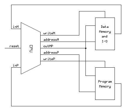
Hack II Computer architecture
Program Memory can be RAM or ROM. If ROM, writes to it are ignored. (Clever programs can determine if they are running in ROM.) Since writes to Data and Program Memory never occur at the same time, they can share a common output bus.
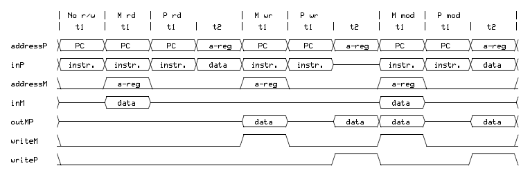
Normal instructions execute in one clock cycle called t1. Instructions that access data in Program
Memory require an extra clock cycle called t2. This timing diagram shows how t2 is inserted
for the Program Memory accesses, and what data is on the various buses at what time.

Hack II CPU timing diagram
The instructions shown are: (No r/w) no memory access, (M rd) Data Memory read, (P rd) Program Memory read,
(M wr) Data Memory write, (P wr) Program Memory write, (M mod) Data Memory modify and
(P mod) Program Memory modify.
When a bus on the timing diagram shows a midline value, the bus's output is undefined or its input value
is unused.
addressM is forced to 0 except during Data Memory accesses. The Hack I computer always puts the
A-register's value on addressM. On Hack II this could result in inadvertent reads from
the Screen and Keyboard when addresses for the upper 16K of Program Memory are present in the
A-register. These reads are benign for the current Hack I/O modules, but that may not be the case
in the future.
--Mark

