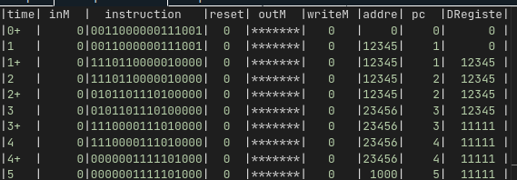
The image above is the top of the compare file for the CPU project in chapter 5.
I'm struggling to justify the timings of the DRegister output.
I can see that when the CPU receives the instruction to store 12345 in the A register, at time 0+, it's not until the rising edge of a clock signal (TOCK) that the register output updates, hence we see 12345 on addressM at time 1. -> this all makes sense to me.
at the next TICK (1+), the CPU receives an instruction to store the contents of the A register in the D register, my assumption is that the input to the D register would be set to 12345 effectively instantaneously, i.e. on 1+, however, as above, the D register output wouldn't read 12345 until the next rising edge clock cycle and 2.
What am I missing, is Dregister value in the file above supposed to actually be the input of the D register?
I've seen a few similar posts ->
http://nand2tetris-questions-and-answers-forum.52.s1.nabble.com/CPU-second-tick-DRegister-output-td4026390.html, this one with a very informative look at hardware, but one post alluding to a potential error in D register in the file.
http://nand2tetris-questions-and-answers-forum.52.s1.nabble.com/CPU-D-Register-Issue-td4027334.html#a4027345

