CMOS ICs are made using
Field Effect Transistors. FETs come in two varieties,
p-channel and
n-channel.
| P-Channel FET | | N-Channel FET |
|---|
|
| source |
| gate | 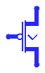 | |
| drain |
| |
| source |
| gate | 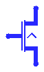 | |
| drain |
|
Simplified for this discussion, the p-channel FET only turns on the connection between the source and the drain when the gate is
low voltage. The n-channel FET only turns on when the gate is high voltage. Otherwise, there is no connection between the source and the drain.
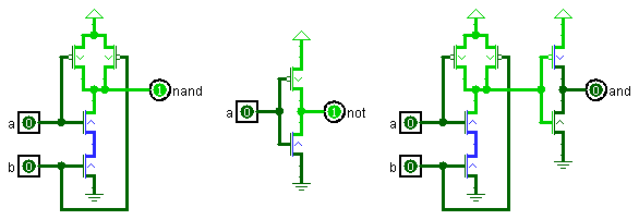
First I'll describe how the Not works. The upper transistor is a P-FET with its source connected to power (+5V) and the lower transistor is an N-FET with its source connected to ground (0V). Both transistors' drains are connected to the Not's output.
When the input to the Not is low, the P-FET is turned on and the N-FET is turned off. The output is only connected to +5V. When the input is high, the P-FET is turned off and the N-FET is turned on. The output is only connected to 0V.
The And also has P-FETs connected to power and N-FETs connected to ground. The P-FETs are connected in parallel and the N-FETs are connected in series.
When either of the inputs is low, one or both of the P-FETs is turned on and one or more of the N-FETs will be turned off. The output is connected only to +5V. When both inputs are high, both P-FETs are turned off and both N-FETs are turned on. The output is only connected to 0V.
Think about this: what happens if we vertically mirror the geometry of the Nand gate so that there are series connected P-FETs on top and parallel connected N-FETs on the bottom? It turns out that it's as easy to make Nor gates as Nand gates in CMOS.
--Mark