Physical implementation of NAND and DFF primitives

classic Classic list List threaded Threaded
17 messages Options
Reply | Threaded
Open this post in threaded view
|

Physical implementation of NAND and DFF primitives

checedrodgers
Hello all,

I am about halfway done with the Nand 2 Tetris course, and I'm enjoying myself immensely. For a long time, I have wanted to understand "the full stack" with regard to computers, and the textbook by Dr. Nisan and Dr. Schocken has made that goal attainable. Many thanks to them for their work.

The textbook shows that an engineer can construct a computer by creatively and intelligently arranging a small set of primitive parts. To my mind, the most important of these primitives are the NAND gate and the Data Flip Flop. If you start with just these two parts, the book will show you how to arrange them into the building blocks necessary to build a functional computer. (The NAND gate is introduced on page 11, and the DFF is introduced on page 42. Also see page 19, where the authors reveal the fascinating fact that any logic gate can be constructed using only NAND gates!)

Because the book assumes that these primitives are already available to a hypothetical computer engineer, it does not go into detail to describe how they are implemented. I decided that I wanted to know how these parts were built in the physical world! Through much trial and error, over the course of about six weeks I was able to contruct a working NAND gate and DFF. I even added an "enable" multiplexer to the DFF to make it a 1-bit register. (See page 43.) I did not use any pre-packaged logic gates in this project; I used only wire, switches, LED's, batteries, resistors, and NPN transistors.

I've uploaded a video to Youtube showing my circuits in operation, as well as my circuit diagrams. I hope this will be interesting and useful to many of you. Enjoy!

https://www.youtube.com/watch?v=8O68_Ovw6j4
Reply | Threaded
Open this post in threaded view
|

Re: Physical implementation of NAND and DFF primitives

cadet1620
Administrator
Congratulations.  That's impressive work.

--Mark
Reply | Threaded
Open this post in threaded view
|

Re: Physical implementation of NAND and DFF primitives

checedrodgers
Thanks very much! I certainly learned a lot.
Reply | Threaded
Open this post in threaded view
|

Re: Physical implementation of NAND and DFF primitives

cadet1620
Administrator
If you are running Windows, you can get a free schematic editor at
    http://expresspcb.com/ExpressPCBHtm/Download.htm
You also get a free PCB layout tool.  (Their intent is that you design your PCB and have them build it...)

Took about a minute to draw your Nor.


Quite handy if you are going to be doing more electronics development.

--Mark
Reply | Threaded
Open this post in threaded view
|

Re: Physical implementation of NAND and DFF primitives

checedrodgers
Wow, that's really neat. I suppose you could prototype on the breadboard, and then use Express PCB to make your circuit permanent.
Reply | Threaded
Open this post in threaded view
|

Re: Physical implementation of NAND and DFF primitives

cadet1620
Administrator
This post was updated on .
I just used the PCB layout program to play around; I've never had one built.  For work, my hardware engineer partners do the layout using professional tools and we have the boards built by regular board houses.

I love playing around with breadboards, especially using them with kids to introduce them to logic ICs.

Here's an adding machine one of my students built.

    TTL adding machine

One of the buttons clears the accumulator and the other one adds the number on the switch to the accumulator.

For those who are curious, here's the schematic:
    adder.pdf

--Mark
Reply | Threaded
Open this post in threaded view
|

Re: Physical implementation of NAND and DFF primitives

checedrodgers
Very, very cool. I'd be interested to look at a diagram of that adder if you have one easily accessible.

So do you teach, or do you do engineering work? You mentioned your hardware engineer coworkers, but then you mentioned a student, so that threw me for a loop. :)
Reply | Threaded
Open this post in threaded view
|

Re: Physical implementation of NAND and DFF primitives

cadet1620
Administrator
I'm an independent contracting firmware / embedded systems programmer.  I also taught high school math to gifted middle school kids for several years (until the school went bankrupt, alas).

I'll add the schematic to the post with the picture.

--Mark
Reply | Threaded
Open this post in threaded view
|

Re: Physical implementation of NAND and DFF primitives

monsonite
Hi All,

I have been doing other things for about a year, but this week had another look at the hardware primitives for the Hack design.

On the breadboard I have a bit slice full-adder based on diode-transistor logic (DTL), which works with data up to around 4MHz frequency. However, allowing for the carry to ripple through 16 stages will probably limit the overall clock to about 250kHz.

The full-adder slice uses 9 NPN transistors, 18 schottky diodes and 18 resistors - effectively built up from 9 DTL NAND gates.

I have also looked at the DFF, and got this down to 5 transistors, 9 diodes and 10 resistors.  It is based on the usual clocked SR flipflop (4 NANDS), with an extra inverter to provide   an inverted version of the data input.

I have tested this at a clock frequency of 200kHz - where if you connect the inverterd ( /Q ) output back to the D input it will act as a divide by 2.

I am working towards a bitslice design of Hack.  Each slice carries the ALU, PC, Address and Memory registers on a convenient sized pcb. (10 x 10 cm - very cheap from dirtypcbs.com)  The pcb also contains LEDs to show register content and programming toggle switches.  16 of these bitslices are stacked together to form the full Hack design.

I estimate that each slice would have approximately 400 components on board  (80 transistors, 160 diodes, 160 resistors) These would be surface mount for compactness.

This was the way computers were built in the mid-1960s.  The 12bit 1965 PDP-8, a DTL design had 1419 transistors & 10418 diodes. There was a lot of circuitry to support the magnetic core memory.


I am using an Arduino to generate the various data and clock signals needed to exercise these circuits.  This allows repetitive test sequences, with timings controlled in the Arduino sketch.  For example, when testing the full-adder slice, the Arduino generated all the 8 possible combinations of A, B and Cin, and I looked at the Sum and Cout  patterns on an oscilloscope.  I hope to further develop this so when it comes to debugging the full ALU, that the Arduino can present a test instruction and test data, and then monitor the ALU outputs for the correct result. I will probably have to use an Arduino Mega to handle all those I/Os

This also leads onto the idea that the Arduino (or other mcu) could be used as the "Memory"  for the final design.  It can easily accept a 16 bit address, look it up in a datatable stored in Flash or external RAM, and produce a 16 bit word. For RAM, it would need an external 64K x16 SRAM connected to 4x8 bit ports.  The Arduino provides a convenient method to get data in and out of the Hack memory - and provide a convenient test/debug and User Interface.  


Ken
Reply | Threaded
Open this post in threaded view
|

Re: Physical implementation of NAND and DFF primitives

monsonite
Here's the schematic and eagleCAD layout of the DFF primitive.

Transistor T1 is the data inverter.

Transistors T2 and T3  NAND the clock with either D or /D

Transistors T4 and T5 are the cross coupled pair that form the flipflop - and produce the outputs Q and /Q

Whilst it looks a lot of components, especially all those double diodes, by using surface mount parts, this reduces to a board area of 1" x 0.75"


Schematic of DTL  D Flipflop using SMT parts


2 Layer PCB for D Flipflop  1" x 0.75"

Reply | Threaded
Open this post in threaded view
|

Re: Physical implementation of NAND and DFF primitives

monsonite
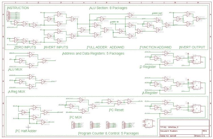
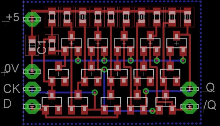
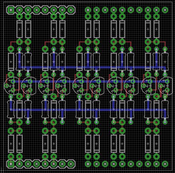
Here is the Bitslice Design.  There are 16 of these connected to a common backplane that carries Address Data and instruction signals.

For convenience, the logic has been grouped into conventional TTL packages eg 74HC00  NAND gates.  That allows an easy assessment to be made of how big this thing is.  Whilst it could be implemented in 74HC00 logic, it could equally well be implemented in discrete DTL or on a FPGA (though bitslice would probably not be appropriate for a FPGA implementation).

The ALU  has two inputs  X (Dreg Out) and Y (A reg or Memory)  and a Carry In bit.  The Carry In connects to the Carry out from the previous slice, or if Slice 0, the Carry In is connected to zero.

The 6 Instruction inputs also connect to the ALU.

ZX   Zero X
NX   Invert X
ZY   Zero Y
NY   Invert Y
F     Function  (select ADD or AND function)
NO  Invert Output

The ALU slice produces a single bit output that goes to the input bit of the D Register, and also a Carry Out.

Every slice performs exactly the same ALU operation given it's Xn, Yn and Cn inputs.


Address and Data Registers

These are identical structures made from a 2 input multiplexer stage and a DFF.


Program Counter

This is somewhat more complicated, as it consists of a half-adder, a register, and the means to reset the register or load it from either the output of the A register or from an incremented version of itself.

A half adder allows the PC to be incremented by 1.  (If this were extended to a full adder, the PC could jump automatically to a given address. Instead this jump address has to be supplied from the Address Register).


As can be seen,  the whole slice is made from just 5 types of circuit configuration:

1.   Half Adder       HA
2.   2 Input MUX    MX
3.   Zeroer             Z
4.   Negater           N
5.   DFF                 D

The structure of these elements when expressed in NAND gates is remarkably similar,   a zeroer is just a special case of a 2 input MUX that can select between zero or the data input,   a Negater is very similar to a half-adder in appearance, and will invert the input bit depending on the control input NX.  It's actually an Exclusive OR made from 4 NAND gates, just like the half-adder.

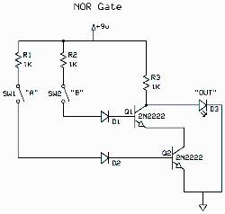
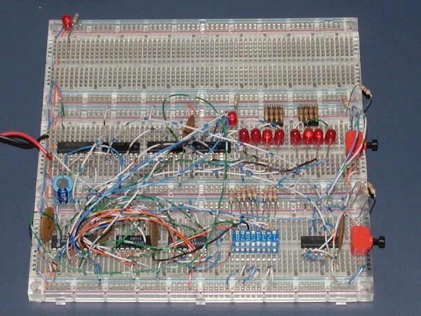
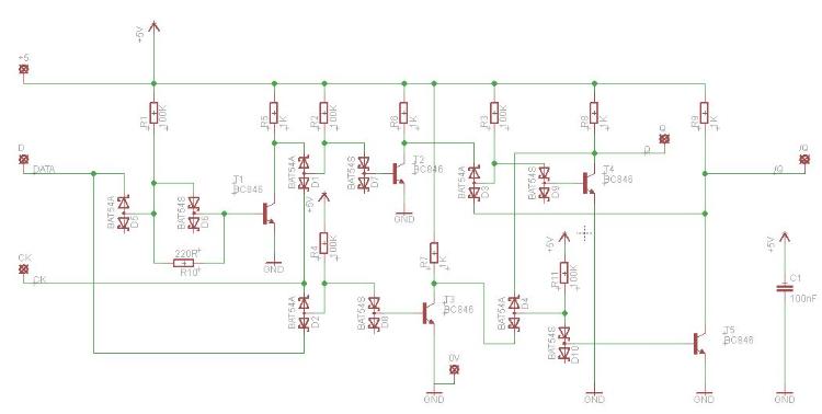
If these elements can be implemented efficiently in logic, whether DTL, TTL, CMOS etc, and be shown to work at high speed without glitches, then just about any computer architecture may be built up from them. It's like having a LEGO set with 5 different colours of blocks.  DTL will run at about 2MHz maximum, and my DFF design needs more tuning of resistor values to get it to clock at much more than 200kHz.
As stated earlier the carry propagation delay through 16 slices (both for the ALU and the PC) can be significant - and this will limit the overall speed that a DTL version of Hack will run at.

A Bitslice Implementation of Hack


Reply | Threaded
Open this post in threaded view
|

Re: Physical implementation of NAND and DFF primitives

cadet1620
Administrator
Cool project!

You can save a few transistors per slice in the ALU by inverting the control signals. Move the 'z*' inverters to the instruction decoder so there are only 3 transistors instead of 3 per slice.

If you invert 'nx' and 'ny' in the instruction decoder, then you can eliminate the output inverter in the "zero" circuit. (Your conditional inverter is an Xor: !a xor b == a xor !b.)

I don't see any mention of the ALU's 'zr' status bit.  You can add a ripple zero detect to your ALU slice: Zout = Zin & !out.  I think transistor count will be the same as an external 16 bit zero detect, but it might be better mechanically.  (Ripple delay shouldn't be a problem since its ripple occurs in parallel with the adder's.)

--Mark
Reply | Threaded
Open this post in threaded view
|

Re: Physical implementation of NAND and DFF primitives

monsonite
Hi Mark

Thanks for the tips. I'll look and see if  I can save transistors in the instruction decoder stage.

Back in the mid 1960's when transistors cost today's equivalent of $10 to $50 it was important to save every last one - thus the amazingly minimal design of the PDP-8.   1400 transistors and 10000 diodes. If you could make the logic work using diodes, and save a transistor here and there - DEC would do it.

However, these days, high speed switching transistors (eg MMBT2369L) are just 5 cents, likewise with high speed schottky diodes. So the design exercise should be put into creating a good DTL NAND  (high speed, good fan-out, low power) rather than saving down to the last transistor.

Likewise with the DFF. It has to be high speed and free of race conditions and glitches. Get these two building blocks right - and you have a good DTL computer.

Amazingly - someone is reverse engineering the PDP-8 logic  modules and offering these designs as EagleCAD board and schematics. What a dedication  to the art.

http://svn.so-much-stuff.com/svn/trunk/Eagle/projects/DEC/Rxxx/R211/R211X.pdf

Will keep you informed with any progress.  I'm 50 this year - and looking at this as a retirement project.


Ken

Reply | Threaded
Open this post in threaded view
|

Re: Physical implementation of NAND and DFF primitives

monsonite
Hi Mark and Forum

Here's a concept I am working on.

It's a 50mm x 50mm  (about 2" x 2") square pcb with 10 2 input DTL NAND gates implemented as a module in conventional through-hole components.  This would allow them to be built by anyone who can do conventional soldering - not just limited to SMT.


The reason for 10 nands, is that it allows one module to be configured as a full adder,  or a DFF plus some register loading logic.

Connection to the module is by way of standard 0.1"  long headers ( as used for stacking shields on Arduino)

They are spaced at 1.8" pitch - so you can put these modules into a pair of adjacent breadboards.  Additionally  I have used an asymmetric header pattern - so you can't get them in backwards and fry the module because +5V and 0V get swapped over!

Using these modules, the bitslice could be done in 8 modules.  Allowing for things like LED driving and  toggle switch input, HACK could be implemented in 160 of these modules, at a cost of about  $2.40 per module.

Cost estimates:

PCB                              $1.00
Transistors (10)            $0.35
Diodes  (30)                 $0.60
Resistors (20)              $0.20
Headers  (4)                 $0.20


Reply | Threaded
Open this post in threaded view
|

Re: Physical implementation of NAND and DFF primitives

monsonite
Hi All,

I have looked more into producing a module that provides the basic building blocks for the N2T design.

I have increased the transistor count from 10 to 12,  with the additional transistors providing the pair of cross-coupled NANDS, as used in the DFF.  This gives much better flexibility - and allows the module to be more easily configured as a DFF, or more correctly a single bit register.

The module has jumper links to allow the various configurations to be set.   Anticipated configurations will be:

1.   Full Adder  (or 2 half adders)
2.   2  XOR   (signal negaters)
3.   2  two input MUX
4.   DFF  plus loading MUX
5    Various combinatorial gates, inverters etc.

I have included a LED on the Q output of the DFF - with a suitably slow clock frequency, this can be used for display or diagnostic purposes.

I am also planning a pin compatible module that uses standard 74HC00 Nands instead of the DTL.  This would allow improved performance, cleaner signals, and a lot less construction involved.

I plan to have a small batch of pcbs manufactured to test the performance of the DTL design.


Ken


Reply | Threaded
Open this post in threaded view
|

Re: Physical implementation of NAND and DFF primitives

checedrodgers
That is fascinating work, Monsonite. Please do keep us updated on any progress. Do you have any plans to implement on-chip memory, or do you think the Arduino is the best way to go?
Reply | Threaded
Open this post in threaded view
|

Re: Physical implementation of NAND and DFF primitives

monsonite
I think it would probably be easier initially to get the Arduino to simulate the memory.

Certainly using a microcontroller as a poorman's logic probe - to check the states of all those gates and latches would make the debugging process easier.

Ultimately  a 64K x 16 SRAM could be wired in - but it would likely need some additional octal latches, read/write steering logic and address decoding hardware to make it work.

Dieter Mueller made an interesting transistor computer - it's worth a look.

http://www.6502.org/users/dieter/mt15/mt15.htm 


Ken