Physical structure of the multi-chips? [CODE SPOILER ALERT]

classic Classic list List threaded Threaded
3 messages Options
Reply | Threaded
Open this post in threaded view
|

Physical structure of the multi-chips? [CODE SPOILER ALERT]

JackH
I wanted to check whether I'm visualizing the multi-chips right. I've got code that works for Not-16, and as far as I can tell there isn't a simpler way to code them than [SPOILER ALERT]:

Nand (a=in[0], b=in[0], out=out[0]);
Nand (a=in[1], b=in[1], out=out[1]);
.
. etc
.
Nand (a=in[15], b=in[15], out=out[15]);

What I wanted to check is how this would actually be laid out on a chip, in case I'm thinking about buses and multi-pins entirely wrong. Would you have a bundle of 16 incoming wires (silicon tracks, or whatever), collectively called pin a[16], which then splits into 16 individual wires, each one passing through its own Nand gate, requiring 16 Nand gates in total. Then the out wires of all the gates recombine into the bundle out[16]. This seems more likely than one Nand gate being able to handle 16 different inputs at the same time, but I couldn't see an explicit description or find a diagram anywhere. Thought I should check that I know what's going on, in case I come away with completely the wrong idea!
Reply | Threaded
Open this post in threaded view
|

Re: Physical structure of the multi-chips? [CODE SPOILER ALERT]

cadet1620
Administrator
There isn't a simpler way in HDL; you must have a Not line for each bit.

You have the right idea about hardware. Whether it's inside an IC or connections between ICs there is a wire for each bit. The signals are usually named individually, for instance DB0, DB1, etc. but are drawn on schematics as heavier lines indicating buses and labeled as such.

Note that the gates for individual bits may not be closely arrayed on the chip, depending on the function of the bus. It might be better for the layout to have them closer to other related circuitry, than to each other.

It is possible to have more than two inputs to a Nand gate, but that makes it an n-way gate, not multi-bit. Not gates often are just 1-input Nand gates.

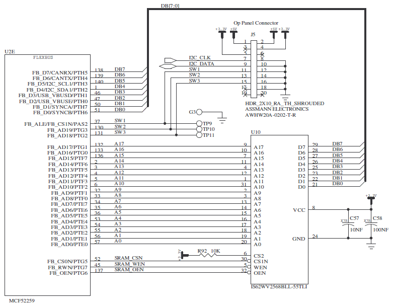
Here's an snippet from the schematic from one of my current projects.
schematic
--Mark
Reply | Threaded
Open this post in threaded view
|

Re: Physical structure of the multi-chips? [CODE SPOILER ALERT]

JackH
Thanks, that's good to know that I wasn't missing something obvious! With Not-16 being pretty much the simplest example possible, and everything else from now on becoming more complex, I wanted to be sure that there actually were that many gates, wires and connections. I'm going to have to simplify my diagrams or they'll be an unreadable mess before too long!