Why won't this work?

classic Classic list List threaded Threaded
2 messages Options
Reply | Threaded
Open this post in threaded view
|

Why won't this work?

glassesfame
CHIP Memory {
    IN in[16], load, address[15];
    OUT out[16];

    PARTS:
    DMux (in=load, sel=address[14], a=ramload, b=device);
    DMux (in=device, sel=address[13], a=screenload, b=keyload);
    RAM16K (in=in, load=ramload, address=address[0…13], out=ram);
    Screen (in=in, load=screenload, address=address[0…12], out=screen);
    Keyboard (out=keyboard);
    Mux16 (a=ram, b=screen, sel=screenload, out=temp);
    Mux16 (a=temp, b=keyboard, sel=keyload, out=out);
}

This is my Memory Chip and I can't see anything wrong with it. However, the Hardware Stimulator is refusing to run it and when I submit it into the grader output, I am told that I have an 'unspecified sub-bus'. I really need some help - the hardware stimulator also refuses to run anything with RAM16K and Screen, is it because I've made some mistake in the code?

For example, this will run:
CHIP copy {

    IN in[16], load, address[15];
    OUT out[16];

    PARTS:
    DMux (in=load, sel=address[14], a=ramload, b=device);
    DMux (in=device, sel=address[13], a=screenload, b=keyload);
    Keyboard (out=data);
    Mux16 (a=in, b=in, sel=screenload, out=temp);
    Mux16 (a=temp, b=data, sel=keyload, out=out);
}

but once I add in one line of Screen (in=in, load=load, address=address[0...12], out=unknown);, it will stop working. Example:

CHIP copy {

    IN in[16], load, address[15];
    OUT out[16];

    PARTS:
    DMux (in=load, sel=address[14], a=ramload, b=device);
    DMux (in=device, sel=address[13], a=screenload, b=keyload);
    Keyboard (out=data11);
    Screen (in=in, load=screenload, address=address[0…12], out=data10);
    Mux16 (a=in, b=data10, sel=screenload, out=temp);
    Mux16 (a=temp, b=data11, sel=keyload, out=out);
}

Please explain?
Reply | Threaded
Open this post in threaded view
|

Re: Why won't this work?

xedover
whoa... I think you need to review the Project 5 slides and book pdf's. The CPU chip was the most difficult for me, and this Memory chip was, I think, the second hardest to get my head around. (and it probably helps to do the CPU first, if you haven't already)

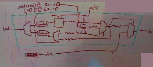
I tried to diagram what you've implemented, and I can't tell what its trying to do. (and when you say "works", for your smaller Chip, Copy -- what exactly do you mean by "works"? In what way does it work?)

Memory chip

To start with, let's looks at slide 5 (or 18)...
Notice that the Memory chip has information flowing both to and from the bus(es). That's what the "load" bit is for, to control when to read and when to write. Now see slide 22-25 (will probably make more sense with the video).

Now, let's look at Dia 5.6 on p17 in the book...
Notice the address space is divided into sections
0-16,383 -- addresses the 16K RAM
16,384-24,575 -- addresses the screen
24576 -- addresses the keyboard

It also shows those same values as Hex:
0x0000-0x5FFF: accessing an address in this range results in accessing the RAM.
0x4000-0x5FFF: accessing an address in this range results in accessing the Screen.
0x6000: accessing this address results in accessing the Keyboard. (anything above in invalid)

But I actually find it easier to view these values in binary:
// 16-bit address [0..15] bx0000 0000 0000 0000 -- not used (reference only)
// 15-bit address [0..14]  bx000 0000 0000 0000 -- this memory chip in/out  0x0000 - 0x7fff
// 14-bit address [0..13]   bx00 0000 0000 0000 -- Ram16k in/out            0x0000 - 0x3fff
// 13-bit address [0..12]    bx0 0000 0000 0000 -- Screen in/out            0x4000 - 0x5fff

//                          0000 0000 0000 0000 -- start                    0x0000 -
//                          0011 1111 1111 1111 --    end                          - 0x3fff
//                          0100 0000 0000 0000 -- start                    0x4000 -
//                          0101 1111 1111 1111 --    end                          - 0x5fff
//  1-bit address ~~~~~~~   0110 0000 0000 0000 -- Keyboard out             0x6000
//                           ^^
//    truth table            00  -- ram16K (low8K)
//   bits 15 and 14          01  -- ram16K (high8K)
//   address[13..14]         10  -- screen
//                           11  -- kbd


Notice bits 14 and 15, looking up the columns, looks like a truth table, no? (think about how to use these to select which sections of memory to read or write to and from.)

Finally, looks at Dia 5.9 on p24 to see how the CPU and Memory chips connect together. Pay attention to the various inputs and outputs and control bits.

I hope this helps.