Question about Figure 3.2, Page 48, Second Edition of the book

classic Classic list List threaded Threaded
16 messages Options
Reply | Threaded
Open this post in threaded view
|

Question about Figure 3.2, Page 48, Second Edition of the book

charleszzx

When studying Figure 3.2, Page 48, Second Edition of the book, I can't understand one particular part of the diagram circled red. If we probe at the transition between Cycle 3 and 4, input and output signals are both 1. However, since the picture shows a NOT gate, shouldn't the input and output signal have opposite values? Thanks for the help!
Reply | Threaded
Open this post in threaded view
|

Re: Question about Figure 3.2, Page 48, Second Edition of the book

rleininger
To me, the response of the Not gate presented in Figure 3.2 seems inconsistent.  I would think the transition to logic 1 that occurs during cycle 3 should produce the same response that is shown in cycle 1.  The change would produce a diagram such as shown below.  But I may be missing something.


Reply | Threaded
Open this post in threaded view
|

Re: Question about Figure 3.2, Page 48, Second Edition of the book

charleszzx
I agree. This is more likely an error in the new edition of the book.
Reply | Threaded
Open this post in threaded view
|

Re: Question about Figure 3.2, Page 48, Second Edition of the book

WBahn
Administrator
I think the point of the figure is to show the effect of the propagation delay through the gate. Say the gate has a propagation delay of 10 ns (just making up a number). When the input to the gate changes, the output won't start changing until about 10 ns after the input changes. So during that time both the input and the output will appear to be the same value.

Reply | Threaded
Open this post in threaded view
|

Re: Question about Figure 3.2, Page 48, Second Edition of the book

charleszzx
If that is the case, does it imply that this particular NOT gate will output the wrong values sometimes?
Reply | Threaded
Open this post in threaded view
|

Re: Question about Figure 3.2, Page 48, Second Edition of the book

WBahn
Administrator
If will if you don't give it time to process its inputs.

Things in the real world do not happen instantly. They take time. Your design has to take this into account by ensuring that there is enough time for all signals to propagate from input to output along all paths (the slowest path is known as the critical path and it drives the design). The critical path sets that maximum clock speed in your system. If you run you system faster than that, you risk capturing values that have not settled to their correct states.
Reply | Threaded
Open this post in threaded view
|

Re: Question about Figure 3.2, Page 48, Second Edition of the book

charleszzx
So can we conclude that the clock speed is not properly designed since we have input=output=1 when we probe the transition between Cycle 3 and 4?
Reply | Threaded
Open this post in threaded view
|

Re: Question about Figure 3.2, Page 48, Second Edition of the book

WBahn
Administrator
No. You can't conclude that. ANY time the input to a logic gate changes, it WILL take a finite amount of time before that change is reflected in the inputs.

A basic logic gate doesn't know anything about clock cycles. Changes in the input are reflected at the output once they have propagated through the circuitry in the gate. That takes a certain amount of time.

What is troubling about that diagram isn't that there is a delay, but why/how the input is changing BEFORE the clock edge. The better representation would be to show the input changing at (or shortly after) a clock edge to reflect the fact that the cause for it to start changing is a change in the output of some register, which happens in conjunction with a clock edge. Then show the output changing slightly later, but being finished and stable before the next clock edge.
Reply | Threaded
Open this post in threaded view
|

Re: Question about Figure 3.2, Page 48, Second Edition of the book

rleininger
In reply to this post by charleszzx
I have now given this question a bit more thought in the clear light of morning.  I agree with WBahn about the purpose of the diagram: to illustrate the need to read the output of combinational gates only after time is allowed for a change in input signal to propagate through the gate to the output.  The outputs of combinational gates are considered valid and to be used only at a specific, regular point in each clock cycle.  Therefore, although combinational circuits do not depend on the clock for their operation, they certainly depend on the clock for their use.  This is made much more clear in several slides provided for Project 3 on the From Nand to Tetris web site which I reproduce below (the slides are snipped from the version revised for the 2nd Ed of the book):

Chapter 3 Slide, 2nd Ed-Slide 17

Chapter 3 Slide, 2nd Ed-Slide 18

Chapter 3 Slide, 2nd Ed-Slide 19

My original complaint was that the Not gate in the diagram shows inconsistent response behavior.  Only in the questioned section does the output response lag behind the input.  In every other case, the input and response occur together.  Such unpredictable behavior would seem to me to be undesirable.
Reply | Threaded
Open this post in threaded view
|

Re: Question about Figure 3.2, Page 48, Second Edition of the book

charleszzx
In reply to this post by WBahn
Thank you so much for the explanation. I did find that part of the diagram a bit confusing. Now I understand it a lot better!
Reply | Threaded
Open this post in threaded view
|

Re: Question about Figure 3.2, Page 48, Second Edition of the book

charleszzx
In reply to this post by rleininger
These slides are helpful. I am starting to think that maybe it makes more sense to shift all vertical green lines half-cycle to the right. By doing this, we are still probing "at a specific, regular point in each clock cycle". Then, if we probe at these new positions, the values make sense.
Reply | Threaded
Open this post in threaded view
|

Re: Question about Figure 3.2, Page 48, Second Edition of the book

WBahn
Administrator
That Slide 18 was poorly thought out.

That they have the input changing slightly before the clock edge in the middle of the slide is annoying, but it's hard to claim it is wrong (the input might be changing because of some external event unrelated to the clock). But the last transition (as well as the transition between 1 & 2) shows the output starting to change before the input has started to change. THAT makes no sense whatsoever (unless the Not gate is psychic).

To be consistent, they need to pick an amount of time (say 10% of a clock cycle) for the delay and then consistently show that the output starts to change that amount of time after the input started to change. A more accurate notion would be that it starts to change one propagation delay after the input changes about half way, but if the transitions are drawn uniformly, this doesn't matter).


Reply | Threaded
Open this post in threaded view
|

Re: Question about Figure 3.2, Page 48, Second Edition of the book

Koki
In reply to this post by charleszzx
The image in this document is incorrect and I believe the image below is correct.

Reply | Threaded
Open this post in threaded view
|

Re: Question about Figure 3.2, Page 48, Second Edition of the book

8bittown
This post was updated on .
I believe the *circled bit specifically in question* in the slide in the original post, and also as a ch. 3 lecture slide (#21 of 100), is correct as published. No shifting in any direction is required to correctly indicate the voltage levels and corresponding data outputs. It is supposed to be a visual aid to help convey both what and why, but it was created by people who already understand what's going on with some low level hardware details that might be necessary for understanding why it looks like that. The best description I've found of it online so far is in Ben Eater's breadboard-built 8-bit computer playlist, but I can't find the specific video at time of comment.

An digital oscillator used as a clock is one way that infinitely-varying analog electronic voltages coming from power sources are directly transformed into exclusively binary, digital data. It is here that waves turn into 1s and 0s. The authors already know how this is done, but you might not, and it helps explain the voltage/input/output graphs.

To create data, a voltage level is gated: it is set at a threshold level. Any voltage below the gate level represents a 0. The voltage only represents a 1 once the voltage has met or exceeded the level of the gate, at which point the voltage is sufficient to trigger a circuit change that discharges the accumulated voltage. In the circled area of the original post, the input voltage at the end of cycle 3 is only beginning to increase, but has not yet met the threshold. This entire time the input signal is still considered to be 0,  and the corresponding output of the Not gate is correctly indicated as 1 during this time. The input only becomes a 1 once it passes the threshold, at which point the Not gate is triggered to output its corresponding 0. The beginning of the cycle is determined by when the accumulated voltage change gets to high enough, not when it first begins to accumulate. (Two of the not-'corrected' images in this thread show levels that appear to inaccurately show the output voltage beginning to change at the same time as the input voltage. That it does not, is one of the interesting things shown by the image.)

An overly simplified, imprecise water/circuit analogy: Place a cup (capacitor) under a faucet spout left open (voltage line). The cup is on a rotating base designed so when the cup is filled with water past a certain point, it tips over, spills all the water down the drain, then the cup rotates pops back up again for a refill. This repeats as long as the faucet is left running, endlessly refiling, spilling, rotating back up. The length from one spill to the next is one full clock cycle. Simple clocks can be built on breadboards with a transistor and a capacitor serving as the role of "electron cup", endlessly filling, emptying, and refilling.

The book's image and the red circled image in the slides are correctly indicating the point at the end of cycle 3 which the cup has just rotated back into the line of the faucet, is staring to refill. The voltage is only beginning to accumulate at the end of clock cycle 3. Cycle 4 is triggered when the cup refills enough to tip/the voltage passes the gate threshold.

So the NOT gate output of an given input 1 can only begin its quick-but-not-instant change to corresponding 0 once the clock input voltage threshold has accumulated enough to trigger the next cycle. That's what is shown in the graphic.
Reply | Threaded
Open this post in threaded view
|

Re: Question about Figure 3.2, Page 48, Second Edition of the book

WBahn
Administrator
Sorry, but the slide in the OP has issues. Consider just the boxed portion:


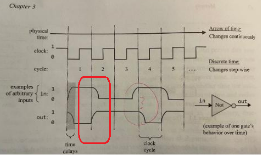
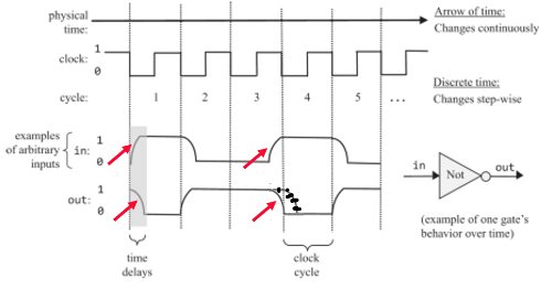
The top is the signal at the input of a Not gate, while the bottom is the output of that same gate.

Notice that the output starts changing immediately at the vertical dashed line (that the line is synched to the clock is immaterial, just use it as a reference point). While the input remains at the same level for a bit and then falls.

Furthermore, the shape of the edges is unreasonable. The rising edge of the output waveform is about what you would expect, namely a rapid initial rise and then tapering off into the final value (these circuits tend to exhibit first-order exponential transitions or close thereto). But the input signal starts off by changing slowing and then accelerates until making an abrupt stop at the final value.

As I noted in a prior post, some of the in/out pairs show reasonable relationships (ignoring the transition shape issue), but others do not. Specifically, the two pairs associated with a falling input require the gate to be psychic.

A note on terminology -- saying that the voltage level is "gated" is not standard terminology (might be a to-English translation issue).

Actual gates have a few defined thresholds.

VinLO -- Voltages below this are guaranteed to be recognized as a logic LO
VinHI -- Voltages above this are guaranteed to be recognized as a logic HI

Voltages in between this are indeterminate. Whether they will be treated as a HI or a LO is not specified or guaranteed. The actual transition point simply somewhere between them and different gates, even on the same integrated circuit, will have different thresholds. Furthermore, the same gate may recognize a particular voltage in this range as a LO today and as a HI tomorrow, just because the chip is at a different temperature.

Similarly, the outputs also have defined ranges.

VoutLO -- The output is guaranteed to be no higher than this when the output is LO and the gate is not being asked to sink more current than it is rated for.
VoutHI -- The output is guaranteed to be no lower than this when the output is HI and the gate is not being asked to source more current than it is rated for.

These limits are designed so that VoutLO is comfortably less than VinLO and, likewise, VoutHI is comfortably higher than VinHI. The differences are the noise margins built into the design.

For CMOS, the actual transition point tends to be pretty close to the midway point because designers like circuits that behave symmetrically. The difference in input voltage between when a specific gate is asserting one level and when it asserts the other level is quite narrow, just a few millivolts or even well under a millivolt in most cases. This is one of the reasons why it is reasonable for timing specifications to be drawn based on the 50% levels of the input and output waveforms, which is the standard practice.


Reply | Threaded
Open this post in threaded view
|

Re: Question about Figure 3.2, Page 48, Second Edition of the book

8bittown
This post was updated on .
It sure looks like the part you have circled might have an issue. My reply above was intended to address OP's part of it, the pen-circled part with the question mark within your image. It appeared to me like this thread was specifically about that part, so I've edited my earlier comment to clarify.

Thanks for the additional helpful info, especially wrt additional real world/physical implementation issues.